- 您现在的位置:买卖IC网 > PDF目录10047 > AD676KNZ (Analog Devices Inc)IC ADC 16BIT 100KSPS 28-DIP PDF资料下载
参数资料
| 型号: | AD676KNZ |
| 厂商: | Analog Devices Inc |
| 文件页数: | 13/16页 |
| 文件大小: | 0K |
| 描述: | IC ADC 16BIT 100KSPS 28-DIP |
| 标准包装: | 1 |
| 位数: | 16 |
| 采样率(每秒): | 100k |
| 数据接口: | 并联 |
| 转换器数目: | 2 |
| 功率耗散(最大): | 480mW |
| 电压电源: | 模拟和数字,双 ± |
| 工作温度: | 0°C ~ 70°C |
| 安装类型: | 通孔 |
| 封装/外壳: | 28-DIP(0.600",15.24mm) |
| 供应商设备封装: | 28-PDIP |
| 包装: | 管件 |
| 输入数目和类型: | 1 个单端,双极 |
AD676
REV. A
–6–
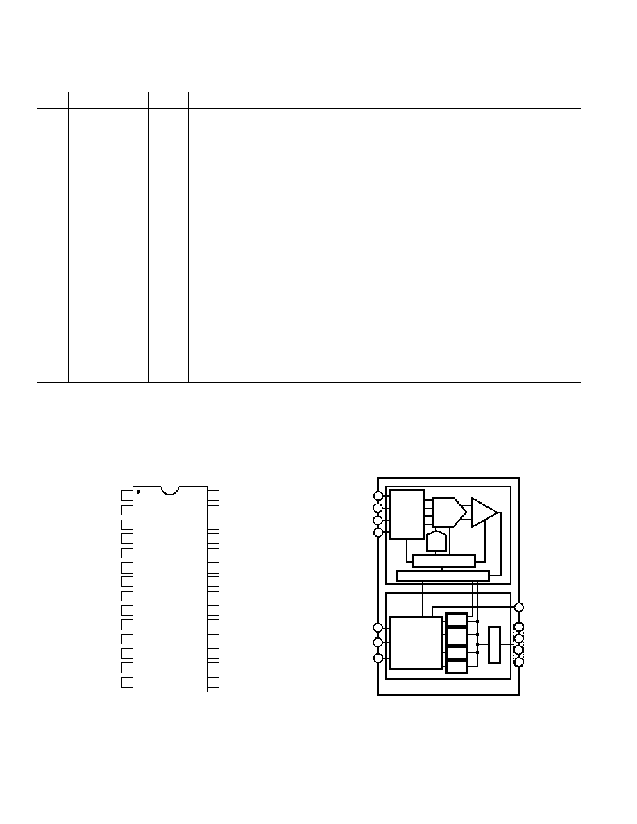
PIN DESCRIPTION
Pin
Name
Type
Description
1–6
BIT 11-BIT 16
DO
BIT 11–BIT 16 represent the six LSBs of data.
7
BUSY
DO
Status Line for Converter. Active HIGH, indicating a conversion or calibration in progress.
BUSY should be buffered when capacitively loaded.
8
CAL
DI
Calibration Control Pin (Asynchronous).
9
SAMPLE
DI
VIN Acquisition Control Pin. Active HIGH. During conversion, SAMPLE controls the state
of the internal sample-hold amplifier and the falling edge initiates conversion (see “Conver-
sion Control” paragraph). During calibration, SAMPLE should be held LOW. If HIGH dur-
ing calibration, diagnostic information will appear on the two LSBs (Pins 5 and 6).
10
CLK
DI
Master Clock Input. The AD676 requires 17 clock cycles to execute a conversion.
11
DGND
P
Digital Ground.
12
VCC
P
+12 V Analog Supply Voltage.
13
AGND
P/AI
Analog Ground.
14
AGND SENSE
AI
Analog Ground Sense.
15
VIN
AI
Analog Input Voltage.
16
VREF
AI
External Voltage Reference Input.
17
VEE
P
–12 V Analog Supply Voltage. Note: the lid of the ceramic package is internally connected to
VEE.
18
VDD
P
+5 V Logic Supply Voltage.
19–28
BIT 1–BIT 10
DO
BIT 1–BIT 10 represent the ten MSB of data.
Type: AI = Analog Input
DI = Digital Input
DO = Digital Output
P = Power
1
2
3
4
5
6
7
8
9
10
11
12
13
14
28
27
26
25
24
23
22
21
20
19
18
17
16
15
TOP VIEW
(Not to Scale)
AD676
BIT 10
BIT 9
BIT 8
BIT 7
BIT 6
BIT 5
BIT 4
BIT 3
BIT 2
BIT 1 (MSB)
VDD
V
EE
V
REF
VIN
BIT 11
BIT 12
BIT 13
BIT 14
BIT 15
BIT 16 (LSB)
BUSY
CAL
SAMPLE
CLK
DGND
VCC
AGND
AGND SENSE
Package Pinout
DIGITAL
CHIP
PAT
GEN
ALU
RAM
MICRO-CODED
CONTROLLER
AGND
AGND SENSE
CAL
SAMPLE
BUSY
COMP
ANALOG
CHIP
16-BIT
DAC
INPUT
BUFFERS
LOGIC & TIMING
CAL
DAC
LEVEL TRANSLATORS
16
BIT 1 – BIT 16
V
IN
VREF
15
14
16
13
8
9
AD676
SAR
1
6
19
28
CLK 10
L
A
T
C
H
7
Functional Block Diagram
相关PDF资料 |
PDF描述 |
|---|---|
| MS3106E28-21PW | CONN PLUG 37POS STRAIGHT W/PINS |
| MS3106E20-29SZ | CONN PLUG 17POS STRAIGHT W/SCKT |
| MS27473T10C99S | CONN PLUG 7POS STRAIGHT W/SCKT |
| IDT72V801L20PF | IC SYNC FIFO 256X9 20NS 64QFP |
| MS27467T21A41S | CONN PLUG 41POS STRAIGHT W/SCKT |
相关代理商/技术参数 |
参数描述 |
|---|---|
| AD676TD | 制造商:未知厂家 制造商全称:未知厂家 功能描述:Analog-to-Digital Converter, 16-Bit |
| AD676TD/883B | 制造商:Analog Devices 功能描述:ADC Single SAR 100ksps 16-bit Parallel 28-Pin CDIP 制造商:Analog Devices 功能描述:ADC SGL SAR 100KSPS 16BIT PARALLEL 28CDIP - Rail/Tube 制造商:Rochester Electronics LLC 功能描述:IC, 16-BIT SAMPLING ADC - Bulk 制造商:Analog Devices Inc. 功能描述:Analog to Digital Converters - ADC 16-Bit Parallel 100 kSPS Sampling |
| AD677 | 制造商:AD 制造商全称:Analog Devices 功能描述:16-Bit 100 kSPS Sampling ADC |
| AD677AD | 功能描述:IC ADC 16BIT SAMPLING 16CDIP RoHS:否 类别:集成电路 (IC) >> 数据采集 - 模数转换器 系列:- 标准包装:1 系列:microPOWER™ 位数:8 采样率(每秒):1M 数据接口:串行,SPI? 转换器数目:1 功率耗散(最大):- 电压电源:模拟和数字 工作温度:-40°C ~ 125°C 安装类型:表面贴装 封装/外壳:24-VFQFN 裸露焊盘 供应商设备封装:24-VQFN 裸露焊盘(4x4) 包装:Digi-Reel® 输入数目和类型:8 个单端,单极 产品目录页面:892 (CN2011-ZH PDF) 其它名称:296-25851-6 |
| AD677BD | 功能描述:IC ADC 16BIT SAMPLING 16-CDIP RoHS:否 类别:集成电路 (IC) >> 数据采集 - 模数转换器 系列:- 产品培训模块:Lead (SnPb) Finish for COTS Obsolescence Mitigation Program 标准包装:250 系列:- 位数:12 采样率(每秒):1.8M 数据接口:并联 转换器数目:1 功率耗散(最大):1.82W 电压电源:模拟和数字 工作温度:-40°C ~ 85°C 安装类型:表面贴装 封装/外壳:48-LQFP 供应商设备封装:48-LQFP(7x7) 包装:管件 输入数目和类型:2 个单端,单极 |
发布紧急采购,3分钟左右您将得到回复。