- 您现在的位置:买卖IC网 > PDF目录10047 > AD676KNZ (Analog Devices Inc)IC ADC 16BIT 100KSPS 28-DIP PDF资料下载
参数资料
| 型号: | AD676KNZ |
| 厂商: | Analog Devices Inc |
| 文件页数: | 4/16页 |
| 文件大小: | 0K |
| 描述: | IC ADC 16BIT 100KSPS 28-DIP |
| 标准包装: | 1 |
| 位数: | 16 |
| 采样率(每秒): | 100k |
| 数据接口: | 并联 |
| 转换器数目: | 2 |
| 功率耗散(最大): | 480mW |
| 电压电源: | 模拟和数字,双 ± |
| 工作温度: | 0°C ~ 70°C |
| 安装类型: | 通孔 |
| 封装/外壳: | 28-DIP(0.600",15.24mm) |
| 供应商设备封装: | 28-PDIP |
| 包装: | 管件 |
| 输入数目和类型: | 1 个单端,双极 |
AD676
REV. A
–12–
AD586 output, thereby optimizing the overall performance of
the AD676. It is recommended that a 10
F to 47 F high qual-
ity tantalum capacitor be tied between the VREF input of the
AD676 and ground to minimize the impedance on the
reference.
+15V
+5V
–15V
100F
AD676
10F
0.1F
78L12
79L12
0.01F
VREF
VDD
VCC
VEE
VIN
VO
NR
GND
10F
0.1F
1F
AD587
10F
15
17
18
12
16
4
2
6
8
VIN
10
10
10
Figure 7.
Using the AD676 with
±10 V input range (V
REF = 10 V) typi-
cally requires
±15 V supplies to drive op amps and the voltage
reference. If
±12 V is not available in the system, regulators
such as 78L12 and 79L12 can be used to provide power for the
AD676. This is also the recommended approach (for any input
range) when the ADC system is subjected to harsh environ-
ments such as where the power supplies are noisy and where
voltage spikes are present. Figure 7 shows an example of such a
system based upon the 10 V AD587 reference, which provides a
300
V LSB. Circuitry for additional protection against power
supply disturbances has been shown. A 100
F capacitor at each
regulator prevents very large voltage spikes from entering the
regulators. Any power line noise which the regulators cannot
eliminate will be further filtered by an RC filter (10
/10 F)
having a –3 dB point at 1.6 kHz. For best results the regulators
should be within a few centimeters of the AD676.
ANALOG INPUT
As previously discussed, the analog input voltage range for the
AD676 is
±V
REF. For purposes of ground drop and common
mode rejection, the VIN and VREF inputs each have their own
ground. VREF is referred to the local analog system ground
(AGND), and VIN is referred to the analog ground sense pin
(AGND SENSE) which allows a remote ground sense for the
input signal.
The AD676 analog inputs (VIN, VREF and AGND SENSE) ex-
hibit dynamic characteristics. When a conversion cycle begins,
each analog input is connected to an internal, discharged 50 pF
capacitor which then charges to the voltage present at the corre-
sponding pin. The capacitor is disconnected when SAMPLE is
taken LOW, and the stored charge is used in the subsequent
conversion. In order to limit the demands placed on the external
source by this high initial charging current, an internal buffer
amplifier is employed between the input and this capacitance for
a few hundred nanoseconds. During this time the input pin ex-
hibits typically 20 k
input resistance, 10 pF input capacitance
and
±40 A bias current. Next, the input is switched directly to
the now precharged capacitor and allowed to fully settle. During
this time the input sees only a 50 pF capacitor. Once the sample
is taken, the input is internally floated so that the external input
source sees a very high input resistance and a parasitic input ca-
pacitance of typically only 2 pF. As a result, the only dominant
input characteristic which must be considered is the high cur-
rent steps which occur when the internal buffers are switched in
and out.
In most cases, these characteristics require the use of an external
op amp to drive the input of the AD676. Care should he taken
with op amp selection; even with modest loading conditions,
most available op amps do not meet the low distortion require-
ments necessary to match the performance capabilities of the
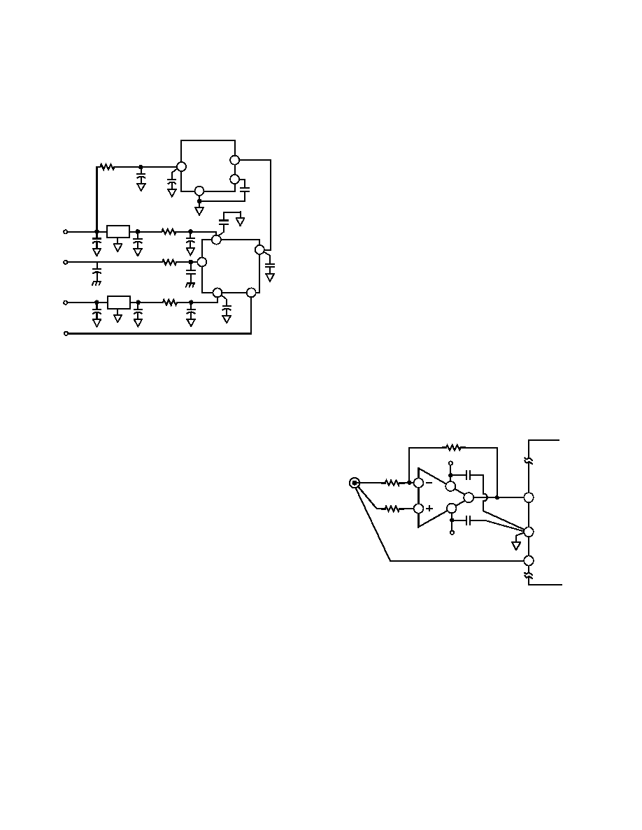
AD676. Figure 8 represents a circuit, based upon the AD845,
recommended for low noise, low distortion ac applications.
For applications optimized more for low bias and low offset than
speed or bandwidth, the AD845 of Figure 8 may be replaced by
the OP27.
499
1k
+12V
–12V
AD845
0.1
F
0.1
F
AGND
SENSE
±5V
INPUT
1k
AD676
15
13
14
2
3
4
7
6
V
IN
Figure 8.
相关PDF资料 |
PDF描述 |
|---|---|
| MS3106E28-21PW | CONN PLUG 37POS STRAIGHT W/PINS |
| MS3106E20-29SZ | CONN PLUG 17POS STRAIGHT W/SCKT |
| MS27473T10C99S | CONN PLUG 7POS STRAIGHT W/SCKT |
| IDT72V801L20PF | IC SYNC FIFO 256X9 20NS 64QFP |
| MS27467T21A41S | CONN PLUG 41POS STRAIGHT W/SCKT |
相关代理商/技术参数 |
参数描述 |
|---|---|
| AD676TD | 制造商:未知厂家 制造商全称:未知厂家 功能描述:Analog-to-Digital Converter, 16-Bit |
| AD676TD/883B | 制造商:Analog Devices 功能描述:ADC Single SAR 100ksps 16-bit Parallel 28-Pin CDIP 制造商:Analog Devices 功能描述:ADC SGL SAR 100KSPS 16BIT PARALLEL 28CDIP - Rail/Tube 制造商:Rochester Electronics LLC 功能描述:IC, 16-BIT SAMPLING ADC - Bulk 制造商:Analog Devices Inc. 功能描述:Analog to Digital Converters - ADC 16-Bit Parallel 100 kSPS Sampling |
| AD677 | 制造商:AD 制造商全称:Analog Devices 功能描述:16-Bit 100 kSPS Sampling ADC |
| AD677AD | 功能描述:IC ADC 16BIT SAMPLING 16CDIP RoHS:否 类别:集成电路 (IC) >> 数据采集 - 模数转换器 系列:- 标准包装:1 系列:microPOWER™ 位数:8 采样率(每秒):1M 数据接口:串行,SPI? 转换器数目:1 功率耗散(最大):- 电压电源:模拟和数字 工作温度:-40°C ~ 125°C 安装类型:表面贴装 封装/外壳:24-VFQFN 裸露焊盘 供应商设备封装:24-VQFN 裸露焊盘(4x4) 包装:Digi-Reel® 输入数目和类型:8 个单端,单极 产品目录页面:892 (CN2011-ZH PDF) 其它名称:296-25851-6 |
| AD677BD | 功能描述:IC ADC 16BIT SAMPLING 16-CDIP RoHS:否 类别:集成电路 (IC) >> 数据采集 - 模数转换器 系列:- 产品培训模块:Lead (SnPb) Finish for COTS Obsolescence Mitigation Program 标准包装:250 系列:- 位数:12 采样率(每秒):1.8M 数据接口:并联 转换器数目:1 功率耗散(最大):1.82W 电压电源:模拟和数字 工作温度:-40°C ~ 85°C 安装类型:表面贴装 封装/外壳:48-LQFP 供应商设备封装:48-LQFP(7x7) 包装:管件 输入数目和类型:2 个单端,单极 |
发布紧急采购,3分钟左右您将得到回复。