- 您现在的位置:买卖IC网 > PDF目录10277 > AD7490BRUZ-REEL7 (Analog Devices Inc)IC ADC 12BIT 16CHAN 28TSSOP PDF资料下载
参数资料
| 型号: | AD7490BRUZ-REEL7 |
| 厂商: | Analog Devices Inc |
| 文件页数: | 18/29页 |
| 文件大小: | 0K |
| 描述: | IC ADC 12BIT 16CHAN 28TSSOP |
| 产品变化通告: | IDD Specification Change 17/Jun/2009 |
| 标准包装: | 1,000 |
| 位数: | 12 |
| 采样率(每秒): | 1M |
| 数据接口: | DSP,MICROWIRE?,QSPI?,串行,SPI? |
| 转换器数目: | 1 |
| 功率耗散(最大): | 12.5mW |
| 电压电源: | 单电源 |
| 工作温度: | -40°C ~ 85°C |
| 安装类型: | 表面贴装 |
| 封装/外壳: | 28-TSSOP(0.173",4.40mm 宽) |
| 供应商设备封装: | 28-TSSOP |
| 包装: | 带卷 (TR) |
| 输入数目和类型: | 16 个单端,单极 |
第1页第2页第3页第4页第5页第6页第7页第8页第9页第10页第11页第12页第13页第14页第15页第16页第17页当前第18页第19页第20页第21页第22页第23页第24页第25页第26页第27页第28页第29页
AD7490
Data Sheet
Rev. D | Page 24 of 28
MICROPROCESSOR INTERFACING
The serial interface on the AD7490 allows the part to be directly
connected to a range of many different microprocessors. This
section explains how to interface the AD7490 with some of the
more common microcontroller and DSP serial interface
protocols.
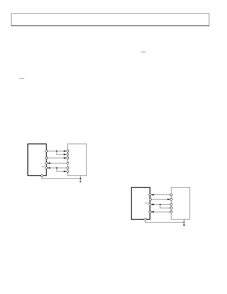
AD7490 to TMS320C541
The serial interface on the TMS320C541 uses a continuous serial
clock and frame synchronization signals to synchronize the data
transfer operations with peripheral devices like the AD7490.
The CS input allows easy interfacing between the TMS320C541
and the AD7490 without any glue logic required. The serial port
of the TMS320C541 is set up to operate in burst mode with
internal CLKX0 (TX serial clock on Serial Port 0) and FSX0
(TX frame sync from Serial Port 0). The serial port control
register (SPC) must have the following setup: FO = 0, FSM = 1,
MCM = 1, and TXM = 1. The connection diagram is shown in
Figure 30. Note that for signal processing applications, it is
imperative that the frame synchronization signal from the
TMS320C541 provide equidistant sampling. The VDRIVE pin
of the AD7490 takes the same supply voltage as that of the
TMS320C541. This allows the ADC to operate at a higher
voltage than the serial interface, that is, TMS320C541, if
necessary.
02691-
029
AD7490
TMS320C541*
SCLK
CLKX
CLKR
DR
DT
FSX
FSR
DOUT
DIN
CS
*ADDITIONAL PINS REMOVED FOR CLARITY
VDRIVE
VDD
Figure 30. Interfacing to the TMS320C541
AD7490 to ADSP-21xx
The ADSP-21xx family of DSPs is interfaced directly to the
AD7490 without any glue logic required. The VDRIVE pin of the
AD7490 takes the same supply voltage as that of the ADSP-
218x.This allows the ADC to operate at a higher voltage than
the serial interface, that is, ADSP-218x, if necessary.
The SPORT0 control register should be set up as follows:
TFSW = RFSW = 1, alternate framing
INVRFS = INVTFS = 1, active low frame signal
DTYPE = 00, right justify data
SLEN = 1111, 16-bit data-words
ISCLK = 1, internal serial clock
TFSR = RFSR = 1, frame every word
IRFS = 0
ITFS = 1
The connection diagram is shown in Figure 31. The ADSP-218x
has the TFS and RFS of the SPORT tied together, with TFS set
as an output and RFS set as an input. The DSP operates in
alternate framing mode, and the SPORT control register is set
up as described. The frame synchronization signal generated on
the TFS is tied to CS, and, as with all signal processing
applications, equidistant sampling is necessary. In this example,
however, the timer interrupt is used to control the sampling rate
of the ADC, and under certain conditions, equidistant sampling
may not be achieved.
The timer register, for example, is loaded with a value that
provides an interrupt at the required sample interval. When an
interrupt is received, a value is transmitted with TFS/DT (ADC
control word). The TFS is used to control the RFS and, thus, the
reading of data. The frequency of the serial clock is set in the
SCLKDIV register. When the instruction to transmit with TFS
is given (that is, AX0 = TX0), the state of the SCLK is checked.
The DSP waits until the SCLK has gone high, low, and high
before transmission starts. If the timer and SCLK values are
chosen such that the instruction to transmit occurs on or near
the rising edge of SCLK, the data may be transmitted or it may
wait until the next clock edge.
For example, if the ADSP-2189 with a 20 MHz crystal has an
overall master clock frequency of 40 MHz, then the master
cycle time is 25 ns. If the SCLKDIV register is loaded with a
value of 3, an SCLK of 5 MHz is obtained, and eight master
clock periods elapse for every 1 SCLK period. Depending on
the throughput rate selected, if the timer registers are loaded
with the value 803, 100.5 SCLKs occur between interrupts and
subsequently between transmit instructions. This situation
results in nonequidistant sampling because the transmit instruc-
tion occurs on a SCLK edge. If the number of SCLKs between
interrupts is a figure of N, equidistant sampling is implemented
by the DSP.
02691-
030
AD7490
ADSP-218x*
SCLK
DR
DT
RFS
TFS
DOUT
DIN
CS
*ADDITIONAL PINS REMOVED FOR CLARITY
VDRIVE
VDD
Figure 31. Interfacing to the ADSP-218x
AD7490 to DSP563xx
The connection diagram in Figure 32 shows how the AD7490
can be connected to the ESSI (synchronous serial interface) of
the DSP563xx family of DSPs from Motorola. Each ESSI (two
on board) is operated in synchronous mode (the SYN bit in
CRB = 1) with internally generated word length frame sync for
both Tx and Rx (FSL1 = 0 and FSL0 = 0 in CRB). Normal
operation of the ESSI is selected by making MOD = 0 in the CRB.
相关PDF资料 |
PDF描述 |
|---|---|
| VI-B1Z-MV-S | CONVERTER MOD DC/DC 2V 60W |
| VI-2N2-MY | CONVERTER MOD DC/DC 15V 50W |
| VI-B51-MW-S | CONVERTER MOD DC/DC 12V 100W |
| AD7490BRUZ-REEL | IC ADC 12BIT 16CHAN 28TSSOP |
| AD7854LARSZ-REEL | IC ADC 12BIT PARALLEL LP 28SSOP |
相关代理商/技术参数 |
参数描述 |
|---|---|
| AD7490SRU-EP-RL7 | 功能描述:模数转换器 - ADC 12-BIT 16CH IC w/ Sequencer RoHS:否 制造商:Analog Devices 通道数量: 结构: 转换速率: 分辨率: 输入类型: 信噪比: 接口类型: 工作电源电压: 最大工作温度: 安装风格: 封装 / 箱体: |
| AD7492 | 制造商:AD 制造商全称:Analog Devices 功能描述:Evaluation Board for 12-bit high speed, low power, successive-approximation ADC |
| AD7492_01 | 制造商:AD 制造商全称:Analog Devices 功能描述:1.25 MSPS, 16 mW Internal REF and CLK, 12-Bit Parallel ADC |
| AD7492AR | 功能描述:IC ADC 12BIT W/REF W/CLK 24-SOIC RoHS:否 类别:集成电路 (IC) >> 数据采集 - 模数转换器 系列:- 标准包装:1,000 系列:- 位数:12 采样率(每秒):300k 数据接口:并联 转换器数目:1 功率耗散(最大):75mW 电压电源:单电源 工作温度:0°C ~ 70°C 安装类型:表面贴装 封装/外壳:24-SOIC(0.295",7.50mm 宽) 供应商设备封装:24-SOIC 包装:带卷 (TR) 输入数目和类型:1 个单端,单极;1 个单端,双极 |
| AD7492AR-5 | 制造商:Analog Devices 功能描述:ADC Single SAR 1.25Msps 12-bit Parallel 24-Pin SOIC W 制造商:Rochester Electronics LLC 功能描述:1.5MSPS 12-BIT ADC, INTERNAL REF + CLOCK - Bulk 制造商:Analog Devices 功能描述:12BIT ADC 1MSPS SMD 7492 SOIC24 |
发布紧急采购,3分钟左右您将得到回复。