- 您现在的位置:买卖IC网 > PDF目录10277 > AD7490BRUZ-REEL7 (Analog Devices Inc)IC ADC 12BIT 16CHAN 28TSSOP PDF资料下载
参数资料
| 型号: | AD7490BRUZ-REEL7 |
| 厂商: | Analog Devices Inc |
| 文件页数: | 9/29页 |
| 文件大小: | 0K |
| 描述: | IC ADC 12BIT 16CHAN 28TSSOP |
| 产品变化通告: | IDD Specification Change 17/Jun/2009 |
| 标准包装: | 1,000 |
| 位数: | 12 |
| 采样率(每秒): | 1M |
| 数据接口: | DSP,MICROWIRE?,QSPI?,串行,SPI? |
| 转换器数目: | 1 |
| 功率耗散(最大): | 12.5mW |
| 电压电源: | 单电源 |
| 工作温度: | -40°C ~ 85°C |
| 安装类型: | 表面贴装 |
| 封装/外壳: | 28-TSSOP(0.173",4.40mm 宽) |
| 供应商设备封装: | 28-TSSOP |
| 包装: | 带卷 (TR) |
| 输入数目和类型: | 16 个单端,单极 |
第1页第2页第3页第4页第5页第6页第7页第8页当前第9页第10页第11页第12页第13页第14页第15页第16页第17页第18页第19页第20页第21页第22页第23页第24页第25页第26页第27页第28页第29页
AD7490
Data Sheet
Rev. D | Page 16 of 28
THEORY OF OPERATION
CIRCUIT INFORMATION
The AD7490 is a fast, 16-channel, 12-bit, single-supply, analog-
to-digital converter. The parts can be operated from a 2.7 V to
5.25 V supply. When operated from a 5 V supply and provided
with a 20 MHz clock, the AD7490 is capable of throughput rates
of up to 1 MSPS.
The AD7490 provides the user with an on-chip, track-and-hold
ADC and a serial interface housed in either a 28-lead TSSOP or
32-lead LFCSP package. The AD7490 has 16 single-ended input
channels with a channel sequencer, allowing the user to select a
sequence of channels through which the ADC can cycle with each
consecutive CS falling edge. The serial clock input accesses data
from the part, controls the transfer of data written to the ADC,
and provides the clock source for the successive approximation
ADC. The analog input range for the AD74790 is 0 V to REFIN
or 0 V to 2 × REFIN, depending on the status of Bit 1 in the
control register. For the 0 V to 2 × REFIN range, the part must be
operated from a 4.75 V to 5.25 V supply.
The AD7490 provides flexible power management options to
allow the user to achieve the best power performance for a
given throughput rate. These options are selected by program-
ming the power management bits in the control register.
CONVERTER OPERATION
The AD7490 is a 12-bit successive approximation ADC based
around a capacitive DAC. The AD7490 can convert analog
input signals in the range 0 V to REFIN or 0 V to 2 × REFIN.
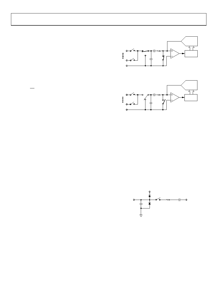
Figure 15 and Figure 16 show simplified schematics of the
ADC. The ADC comprises control logic, SAR, and a capacitive
DAC, which are used to add and subtract fixed amounts of
charge from the sampling capacitor to bring the comparator
back into a balanced condition. Figure 15 shows the ADC
during its acquisition phase. SW2 is closed and SW1 is in
Position A. The comparator is held in a balanced condition,
and the sampling capacitor acquires the signal on the selected
VIN channel.
When the ADC starts a conversion (see Figure 16), SW2 opens
and SW1 moves to Position B, causing the comparator to become
unbalanced. The control logic and the capacitive DAC are used
to add and subtract fixed amounts of charge from the sampling
capacitor to bring the comparator back into a balanced condi-
tion. When the comparator is rebalanced, the conversion is
complete. The control logic generates the ADC output code.
Figure 18 shows the ADC transfer function.
02691-
014
VIN0
VIN15
AGND
A
B
SW1
SW2
4k
COMPARATOR
CAPACITIVE
DAC
CONTROL
LOGIC
Figure 15. ADC Acquisition Phase
02691-
015
VIN0
VIN15
AGND
A
B
SW1
SW2
4k
COMPARATOR
CAPACITIVE
DAC
CONTROL
LOGIC
Figure 16. ADC Conversion Phase
Analog Input
Figure 17 shows an equivalent circuit of the analog input struc-
ture of the AD7490. The two diodes, D1 and D2, provide ESD
protection for the analog inputs. Care must be taken to ensure
that the analog input signal never exceeds the supply rails by
more than 200 mV. This causes these diodes to become forward
biased and to start conducting current into the substrate. The
maximum current these diodes can conduct without causing
irreversible damage to the part is 10 mA. Capacitor C1 in Figure 17
is typically about 4 pF and can primarily be attributed to pin
capacitance. Resistor R1 is a lumped component made up of the
on resistance of a track-and-hold switch and includes the on
resistance of the input multiplexer. The total resistance is typically
about 400 . Capacitor C2 is the ADC sampling capacitor and
typically has a capacitance of 30 pF.
02691-
016
C1
4pF
VIN
CONVERSION PHASE—SWITCH OPEN
TRACK PHASE—SWITCH CLOSED
VDD
R1
C2
30pF
D2
D1
Figure 17. Equivalent Analog Input Circuit
For ac applications, removing high frequency components from
the analog input signal is recommended by use of an RC low-
pass filter on the relevant analog input pin. In applications where
harmonic distortion and signal-to-noise ratio are critical, the
analog input should be driven from a low impedance source.
Large source impedances significantly affect the ac performance
of the ADC. This may necessitate the use of an input buffer
amplifier. The choice of the op amp is a function of the particular
application.
相关PDF资料 |
PDF描述 |
|---|---|
| VI-B1Z-MV-S | CONVERTER MOD DC/DC 2V 60W |
| VI-2N2-MY | CONVERTER MOD DC/DC 15V 50W |
| VI-B51-MW-S | CONVERTER MOD DC/DC 12V 100W |
| AD7490BRUZ-REEL | IC ADC 12BIT 16CHAN 28TSSOP |
| AD7854LARSZ-REEL | IC ADC 12BIT PARALLEL LP 28SSOP |
相关代理商/技术参数 |
参数描述 |
|---|---|
| AD7490SRU-EP-RL7 | 功能描述:模数转换器 - ADC 12-BIT 16CH IC w/ Sequencer RoHS:否 制造商:Analog Devices 通道数量: 结构: 转换速率: 分辨率: 输入类型: 信噪比: 接口类型: 工作电源电压: 最大工作温度: 安装风格: 封装 / 箱体: |
| AD7492 | 制造商:AD 制造商全称:Analog Devices 功能描述:Evaluation Board for 12-bit high speed, low power, successive-approximation ADC |
| AD7492_01 | 制造商:AD 制造商全称:Analog Devices 功能描述:1.25 MSPS, 16 mW Internal REF and CLK, 12-Bit Parallel ADC |
| AD7492AR | 功能描述:IC ADC 12BIT W/REF W/CLK 24-SOIC RoHS:否 类别:集成电路 (IC) >> 数据采集 - 模数转换器 系列:- 标准包装:1,000 系列:- 位数:12 采样率(每秒):300k 数据接口:并联 转换器数目:1 功率耗散(最大):75mW 电压电源:单电源 工作温度:0°C ~ 70°C 安装类型:表面贴装 封装/外壳:24-SOIC(0.295",7.50mm 宽) 供应商设备封装:24-SOIC 包装:带卷 (TR) 输入数目和类型:1 个单端,单极;1 个单端,双极 |
| AD7492AR-5 | 制造商:Analog Devices 功能描述:ADC Single SAR 1.25Msps 12-bit Parallel 24-Pin SOIC W 制造商:Rochester Electronics LLC 功能描述:1.5MSPS 12-BIT ADC, INTERNAL REF + CLOCK - Bulk 制造商:Analog Devices 功能描述:12BIT ADC 1MSPS SMD 7492 SOIC24 |
发布紧急采购,3分钟左右您将得到回复。