- 您现在的位置:买卖IC网 > PDF目录10277 > AD7490BRUZ-REEL7 (Analog Devices Inc)IC ADC 12BIT 16CHAN 28TSSOP PDF资料下载
参数资料
| 型号: | AD7490BRUZ-REEL7 |
| 厂商: | Analog Devices Inc |
| 文件页数: | 28/29页 |
| 文件大小: | 0K |
| 描述: | IC ADC 12BIT 16CHAN 28TSSOP |
| 产品变化通告: | IDD Specification Change 17/Jun/2009 |
| 标准包装: | 1,000 |
| 位数: | 12 |
| 采样率(每秒): | 1M |
| 数据接口: | DSP,MICROWIRE?,QSPI?,串行,SPI? |
| 转换器数目: | 1 |
| 功率耗散(最大): | 12.5mW |
| 电压电源: | 单电源 |
| 工作温度: | -40°C ~ 85°C |
| 安装类型: | 表面贴装 |
| 封装/外壳: | 28-TSSOP(0.173",4.40mm 宽) |
| 供应商设备封装: | 28-TSSOP |
| 包装: | 带卷 (TR) |
| 输入数目和类型: | 16 个单端,单极 |
第1页第2页第3页第4页第5页第6页第7页第8页第9页第10页第11页第12页第13页第14页第15页第16页第17页第18页第19页第20页第21页第22页第23页第24页第25页第26页第27页当前第28页第29页
Data Sheet
AD7490
Rev. D | Page 7 of 28
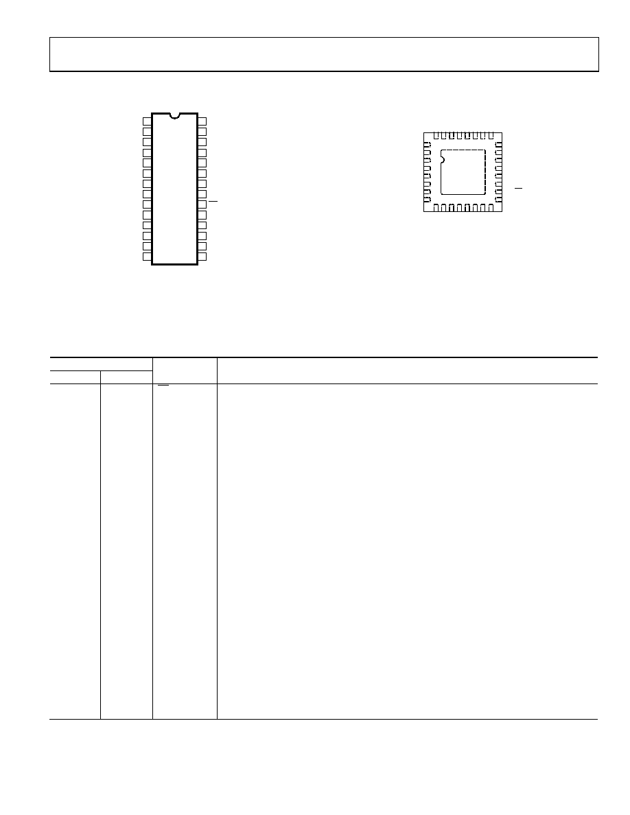
PIN CONFIGURATIONS AND FUNCTION DESCRIPTIONS
02691-
003
AD7490
TOP VIEW
(Not to Scale)
VIN11 1
VIN12
28
VIN10 2
VIN13
27
VIN9 3
VIN14
26
NC
4
VIN15
25
VIN8 5
AGND
24
VIN7 6
REFIN
23
VIN6 7
VDD
22
VIN5 8
AGND
21
VIN4 9
CS
20
VIN3 10
DIN
19
VIN2 11
NC
18
VIN1 12
VDRIVE
17
VIN0 13
SCLK
16
AGND 14
DOUT
15
NC = NO CONNECT
ALL NC PINS SHOULD BE
CONNECTED STRAIGHT TO AGND
Figure 3. 28-Lead TSSOP Pin Configuration
02691-
032
NOTES
1. NC = NO CONNECT. ALL NC PINS
SHOULD BE CONNECTED STRAIGHT
TO AGND.
2. CONNECT EXPOSED PAD TO GND
AD7490
TOP VIEW
(Not to Scale)
1
VIN15
2
NC
3
AGND
4
REFIN
5
VDD
6
AGND
7
CS
8
DIN
24
23
22
21
20
19
18
17
NC
VIN8
VIN7
VIN6
VIN5
VIN4
VIN3
NC
9
10
11
12
13
14
15
16
V
IN
2
V
IN
1
V
IN
0
AG
ND
DO
UT
S
CL
K
V
DRI
V
E
NC
32
31
30
29
28
27
26
25
NC
V
IN
9
V
IN
10
V
IN
11
V
IN
12
V
IN
13
V
IN
14
NC
Figure 4. 32-Lead LFCSP Pin Configuration
Table 4. Pin Function Descriptions
Pin No.
Mnemonic
Description
TSSOP
LFCSP
20
18
CS
Chip Select. Active low logic input. This input provides the dual function of initiating
conversions on the AD7490 and also frames the serial data transfer.
23
21
REFIN
Reference Input for the AD7490. An external reference must be applied to this input. The
voltage range for the external reference is 2.5 V ± 1% for specified performance.
22
20
VDD
Power Supply Input. The VDD range for the AD7490 is from 2.7 V to 5.25 V. For the 0 V to 2 × REFIN
range, VDD should be from 4.75 V to 5.25 V.
14, 21, 24
12, 19, 22
AGND
Analog Ground. Ground reference point for all circuitry on the AD7490. All analog/digital input
signals and any external reference signal should be referred to this AGND voltage. All AGND pins
should be connected together.
13 to 5,
3 to 1,
28 to 25
11 to 9,
7 to 2,
31 to 26,
24
VIN0 to VIN15
Analog Input 0 through Analog Input 15. Sixteen single-ended analog input channels that are
multiplexed into the on chip track-and-hold. The analog input channel to be converted is
selected by using the address bits ADD3 through ADD0 of the control register. The address bits,
in conjunction with the SEQ and SHADOW bits, allow the sequence register to be programmed.
The input range for all input channels can extend from 0 V to REFIN or 0 V to 2 × REFIN as selected
via the RANGE bit in the control register. Any unused input channels should be connected to
AGND to avoid noise pickup.
19
17
DIN
Data In. Logic input. Data to be written to the control register of the AD7490 is provided on this
input and is clocked into the register on the falling edge of SCLK (see the Control Register
section).
15
13
DOUT
Data Out. Logic output. The conversion result from the AD7490 is provided on this output as a
serial data stream. The bits are clocked out on the falling edge of the SCLK input. The data
stream consists of four address bits indicating which channel the conversion result corresponds
to, followed by the 12 bits of conversion data, which is provided by MSB first. The output coding
can be selected as straight binary or twos complement via the CODING bit in the control
register.
16
14
SCLK
Serial Clock. Logic input. SCLK provides the serial clock for accessing data from the part. This
clock input is also used as the clock source for the conversion process of the AD7490.
17
15
VDRIVE
Logic Power Supply Input. The voltage supplied at this pin determines at what voltage the serial
interface of the AD7490 operates.
N/A
EP
EPAD
Exposed Pad. Connect exposed pad to GND.
相关PDF资料 |
PDF描述 |
|---|---|
| VI-B1Z-MV-S | CONVERTER MOD DC/DC 2V 60W |
| VI-2N2-MY | CONVERTER MOD DC/DC 15V 50W |
| VI-B51-MW-S | CONVERTER MOD DC/DC 12V 100W |
| AD7490BRUZ-REEL | IC ADC 12BIT 16CHAN 28TSSOP |
| AD7854LARSZ-REEL | IC ADC 12BIT PARALLEL LP 28SSOP |
相关代理商/技术参数 |
参数描述 |
|---|---|
| AD7490SRU-EP-RL7 | 功能描述:模数转换器 - ADC 12-BIT 16CH IC w/ Sequencer RoHS:否 制造商:Analog Devices 通道数量: 结构: 转换速率: 分辨率: 输入类型: 信噪比: 接口类型: 工作电源电压: 最大工作温度: 安装风格: 封装 / 箱体: |
| AD7492 | 制造商:AD 制造商全称:Analog Devices 功能描述:Evaluation Board for 12-bit high speed, low power, successive-approximation ADC |
| AD7492_01 | 制造商:AD 制造商全称:Analog Devices 功能描述:1.25 MSPS, 16 mW Internal REF and CLK, 12-Bit Parallel ADC |
| AD7492AR | 功能描述:IC ADC 12BIT W/REF W/CLK 24-SOIC RoHS:否 类别:集成电路 (IC) >> 数据采集 - 模数转换器 系列:- 标准包装:1,000 系列:- 位数:12 采样率(每秒):300k 数据接口:并联 转换器数目:1 功率耗散(最大):75mW 电压电源:单电源 工作温度:0°C ~ 70°C 安装类型:表面贴装 封装/外壳:24-SOIC(0.295",7.50mm 宽) 供应商设备封装:24-SOIC 包装:带卷 (TR) 输入数目和类型:1 个单端,单极;1 个单端,双极 |
| AD7492AR-5 | 制造商:Analog Devices 功能描述:ADC Single SAR 1.25Msps 12-bit Parallel 24-Pin SOIC W 制造商:Rochester Electronics LLC 功能描述:1.5MSPS 12-BIT ADC, INTERNAL REF + CLOCK - Bulk 制造商:Analog Devices 功能描述:12BIT ADC 1MSPS SMD 7492 SOIC24 |
发布紧急采购,3分钟左右您将得到回复。