参数资料
| 型号: | AD7606BSTZ-4RL |
| 厂商: | Analog Devices Inc |
| 文件页数: | 18/36页 |
| 文件大小: | 0K |
| 描述: | IC DAS W/ADC 16BIT 64LQFP |
| 设计资源: | Layout Considerations for an Expandable Multichannel Simultaneous Sampling Data Acquisition System Based on AD7606 (CN0148) |
| 标准包装: | 1 |
| 类型: | 数据采集系统(DAS),ADC |
| 分辨率(位): | 16 b |
| 采样率(每秒): | 200k |
| 数据接口: | DSP,MICROWIRE?,并联,QSPI?,串行,SPI? |
| 电压电源: | 模拟和数字 |
| 电源电压: | 2.3 V ~ 5.25 V,4.75 V ~ 5.25 V |
| 工作温度: | -40°C ~ 85°C |
| 安装类型: | 表面贴装 |
| 封装/外壳: | 64-LQFP |
| 供应商设备封装: | 64-LQFP(10x10) |
| 包装: | 标准包装 |
| 其它名称: | AD7606BSTZ-4RLDKR |
第1页第2页第3页第4页第5页第6页第7页第8页第9页第10页第11页第12页第13页第14页第15页第16页第17页当前第18页第19页第20页第21页第22页第23页第24页第25页第26页第27页第28页第29页第30页第31页第32页第33页第34页第35页第36页
Data Sheet
AD7606/AD7606-6/AD7606-4
Rev. C | Page 25 of 36
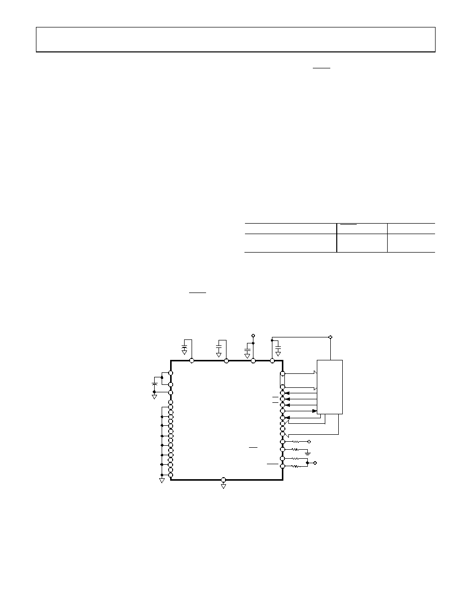
TYPICAL CONNECTION DIAGRAM
Figure 43 shows the typical connection diagram for the AD7606/
AD7606-6/AD7606-4. There are four AVCC supply pins on the
part, and each of the four pins should be decoupled using a 100 nF
capacitor at each supply pin and a 10 F capacitor at the supply
source. The AD7606/AD7606-6/AD7606-4 can operate with the
internal reference or an externally applied reference. In this
configuration, the AD7606 is configured to operate with the
internal reference. When using a single AD7606/AD7606-6/
AD7606-4 device on the board, the REFIN/REFOUT pin
should be decoupled with a 10 F capacitor. Refer to the
Internal/External Reference section when using an application
with multiple AD7606/AD7606-6/AD7606-4 devices. The
REFCAPA and REFCAPB pins are shorted together and
decoupled with a 10 F ceramic capacitor.
The VDRIVE supply is connected to the same supply as the
processor. The VDRIVE voltage controls the voltage value of the
output logic signals. For layout, decoupling, and grounding
hints, see the Layout Guidelines section.
After supplies are applied to the AD7606/AD7606-6/AD7606-4,
a reset should be applied to the AD7606/AD7606-6/AD7606-4
to ensure that it is configured for the correct mode of operation.
POWER-DOWN MODES
Two power-down modes are available on the AD7606/AD7606-6/
AD7606-4: standby mode and shutdown mode. The STBY pin
controls whether the AD7606/AD7606-6/AD7606-4 are in
normal mode or in one of the two power-down modes.
The power-down mode is selected through the state of the
RANGE pin when the STBY pin is low. Table 7 shows the
configurations required to choose the desired power-down mode.
When the AD7606/AD7606-6/AD7606-4 are placed in standby
mode, the current consumption is 8 mA maximum and power-
up time is approximately 100 s because the capacitor on the
REFCAPA and REFCAPB pins must charge up. In standby mode,
the on-chip reference and regulators remain powered up, and
the amplifiers and ADC core are powered down.
When the AD7606/AD7606-6/AD7606-4 are placed in shutdown
mode, the current consumption is 6 A maximum and power-up
time is approximately 13 ms (external reference mode). In shut-
down mode, all circuitry is powered down. When the AD7606/
AD7606-6/AD7606-4 are powered up from shutdown mode,
a RESET signal must be applied to the AD7606/AD7606-6/
AD7606-4 after the required power-up time has elapsed.
Table 7. Power-Down Mode Selection
Power-Down Mode
STBY
RANGE
Standby
0
1
Shutdown
0
AVCC
AGND
VDRIVE
+
REFIN/REFOUT
DB0 TO DB15
CONVST A, CONVST B
CS
RD
BUSY
RESET
AD7606
1F
10F
100nF
DIGITAL SUPPLY
VOLTAGE +2.3V TO +5.25V
ANALOG SUPPLY
VOLTAGE 5V1
EIGHT ANALOG
INPUTS V1 TO V8
PARALLEL
INTERFACE
1DECOUPLING SHOWN ON THE AVCC PIN APPLIES TO EACH AVCC PIN (PIN 1, PIN 37, PIN 38, PIN 48).
DECOUPLING CAPACITOR CAN BE SHARED BETWEEN AVCC PIN 37 AND PIN 38.
2DECOUPLING SHOWN ON THE REGCAP PIN APPLIES TO EACH REGCAP PIN (PIN 36, PIN 39).
REGCAP2
+
10F
REFCAPA
REFCAPB
OS 2
OS 1
OS 0
OVERSAMPLING
100nF
V1
PAR/SER SEL
STBY
REF SELECT
RANGE
V2
V3
V4
V5
V6
V7
V8
REFGND
V1GND
V2GND
V3GND
V4GND
V5GND
V6GND
V7GND
V8GND
VDRIVE
08479-
041
M
ICRO
P
RO
CE
S
O
R/
M
ICRO
CO
NV
E
RT
E
R/
DS
P
Figure 43. AD7606 Typical Connection Diagram
相关PDF资料 |
PDF描述 |
|---|---|
| MS3124E12-10SW | CONN RCPT 10POS JAM NUT W/SCKT |
| V110A8M200BG | CONVERTER MOD DC/DC 8V 200W |
| MS27473E18B30P | CONN PLUG 30POS STRAIGHT W/PINS |
| V110A8M200BF3 | CONVERTER MOD DC/DC 8V 200W |
| M83723/77R1412N | CONN PLUG 12POS STRAIGHT W/SCKT |
相关代理商/技术参数 |
参数描述 |
|---|---|
| AD7606BSTZ-6 | 功能描述:IC DAS W/ADC 16BIT 6CH 64LQFP RoHS:是 类别:集成电路 (IC) >> 数据采集 - ADCs/DAC - 专用型 系列:- 产品培训模块:Lead (SnPb) Finish for COTS Obsolescence Mitigation Program 标准包装:50 系列:- 类型:数据采集系统(DAS) 分辨率(位):16 b 采样率(每秒):21.94k 数据接口:MICROWIRE?,QSPI?,串行,SPI? 电压电源:模拟和数字 电源电压:1.8 V ~ 3.6 V 工作温度:-40°C ~ 85°C 安装类型:表面贴装 封装/外壳:40-WFQFN 裸露焊盘 供应商设备封装:40-TQFN-EP(6x6) 包装:托盘 |
| AD7606BSTZ-6RL | 功能描述:IC DAS W/ADC 16BIT 64LQFP RoHS:是 类别:集成电路 (IC) >> 数据采集 - ADCs/DAC - 专用型 系列:- 产品培训模块:Lead (SnPb) Finish for COTS Obsolescence Mitigation Program 标准包装:50 系列:- 类型:数据采集系统(DAS) 分辨率(位):16 b 采样率(每秒):21.94k 数据接口:MICROWIRE?,QSPI?,串行,SPI? 电压电源:模拟和数字 电源电压:1.8 V ~ 3.6 V 工作温度:-40°C ~ 85°C 安装类型:表面贴装 封装/外壳:40-WFQFN 裸露焊盘 供应商设备封装:40-TQFN-EP(6x6) 包装:托盘 |
| AD7606BSTZ-RL | 功能描述:IC DAS W/ADC 16BIT 64LQFP RoHS:是 类别:集成电路 (IC) >> 数据采集 - ADCs/DAC - 专用型 系列:- 产品培训模块:Lead (SnPb) Finish for COTS Obsolescence Mitigation Program 标准包装:50 系列:- 类型:数据采集系统(DAS) 分辨率(位):16 b 采样率(每秒):21.94k 数据接口:MICROWIRE?,QSPI?,串行,SPI? 电压电源:模拟和数字 电源电压:1.8 V ~ 3.6 V 工作温度:-40°C ~ 85°C 安装类型:表面贴装 封装/外壳:40-WFQFN 裸露焊盘 供应商设备封装:40-TQFN-EP(6x6) 包装:托盘 |
| AD7607 | 制造商:AD 制造商全称:Analog Devices 功能描述:8-Channel Differential DAS with 18-Bit, Bipolar, Simultaneous Sampling ADC |
| AD7607BSTZ | 功能描述:IC DAS W/ADC 14BIT 8CH 64LQFP RoHS:是 类别:集成电路 (IC) >> 数据采集 - ADCs/DAC - 专用型 系列:- 产品培训模块:Lead (SnPb) Finish for COTS Obsolescence Mitigation Program 标准包装:50 系列:- 类型:数据采集系统(DAS) 分辨率(位):16 b 采样率(每秒):21.94k 数据接口:MICROWIRE?,QSPI?,串行,SPI? 电压电源:模拟和数字 电源电压:1.8 V ~ 3.6 V 工作温度:-40°C ~ 85°C 安装类型:表面贴装 封装/外壳:40-WFQFN 裸露焊盘 供应商设备封装:40-TQFN-EP(6x6) 包装:托盘 |
发布紧急采购,3分钟左右您将得到回复。