参数资料
| 型号: | AD7606BSTZ-4RL |
| 厂商: | Analog Devices Inc |
| 文件页数: | 20/36页 |
| 文件大小: | 0K |
| 描述: | IC DAS W/ADC 16BIT 64LQFP |
| 设计资源: | Layout Considerations for an Expandable Multichannel Simultaneous Sampling Data Acquisition System Based on AD7606 (CN0148) |
| 标准包装: | 1 |
| 类型: | 数据采集系统(DAS),ADC |
| 分辨率(位): | 16 b |
| 采样率(每秒): | 200k |
| 数据接口: | DSP,MICROWIRE?,并联,QSPI?,串行,SPI? |
| 电压电源: | 模拟和数字 |
| 电源电压: | 2.3 V ~ 5.25 V,4.75 V ~ 5.25 V |
| 工作温度: | -40°C ~ 85°C |
| 安装类型: | 表面贴装 |
| 封装/外壳: | 64-LQFP |
| 供应商设备封装: | 64-LQFP(10x10) |
| 包装: | 标准包装 |
| 其它名称: | AD7606BSTZ-4RLDKR |
第1页第2页第3页第4页第5页第6页第7页第8页第9页第10页第11页第12页第13页第14页第15页第16页第17页第18页第19页当前第20页第21页第22页第23页第24页第25页第26页第27页第28页第29页第30页第31页第32页第33页第34页第35页第36页
Data Sheet
AD7606/AD7606-6/AD7606-4
Rev. C | Page 27 of 36
DIGITAL INTERFACE
The AD7606/AD7606-6/AD7606-4 provide three interface
options: a parallel interface, a high speed serial interface, and
a parallel byte interface. The required interface mode is selected
via the PAR/SER/BYTE SEL and DB15/BYTE SEL pins.
Table 8. Interface Mode Selection
PAR/SER/BYTE SEL
DB15
Interface Mode
0
Parallel interface mode
1
0
Serial interface mode
1
Parallel byte interface mode
Operation of the interface modes is discussed in the following
sections.
PARALLEL INTERFACE (PAR/SER/BYTE SEL = 0)
Data can be read from the AD7606/AD7606-6/AD7606-4 via
the parallel data bus with standard CS and RD signals. To read the
data over the parallel bus, the PAR/SER/BYTE SEL pin should
be tied low. The CS and RD input signals are internally gated to
enable the conversion result onto the data bus. The data lines,
DB15 to DB0, leave their high impedance state when both CS
and RD are logic low.
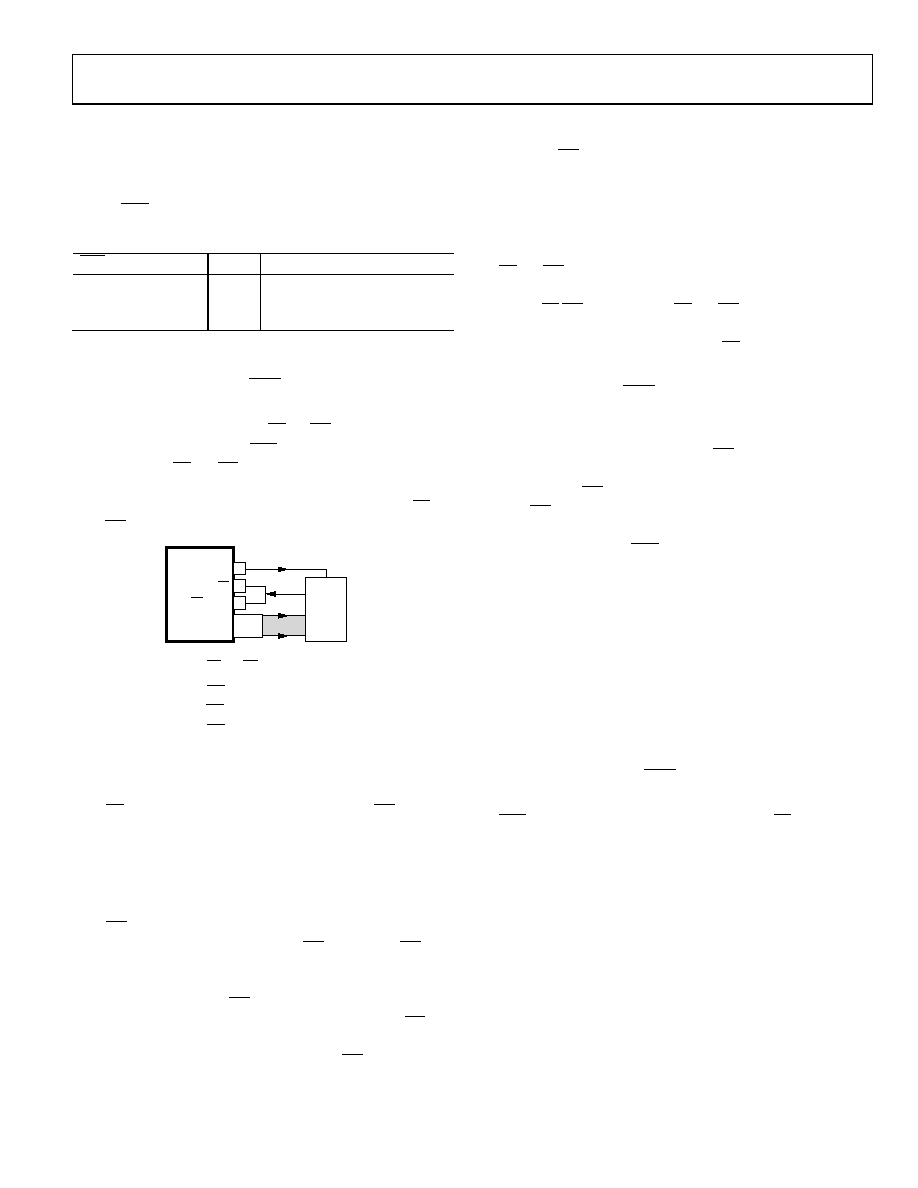
AD7606
14
BUSY
12
RD/SCLK
[33:24]
[22:16]
DB[15:0]
13
CS
DIGITAL
HOST
INTERRUPT
08479-
043
Figure 45. AD7606 Interface Diagram—One AD7606 Using the Parallel Bus,
with CS and RD Shorted Together
The rising edge of the CS input signal three-states the bus, and
the falling edge of the CS input signal takes the bus out of the
high impedance state. CS is the control signal that enables the
data lines; it is the function that allows multiple AD7606/
AD7606-6/ AD7606-4 devices to share the same parallel
data bus.
The CS signal can be permanently tied low, and the RD signal
can be used to access the conversion results as shown in Figure 4.
A read operation of new data can take place after the BUSY
signal goes low (see Figure 2); or, alternatively, a read operation
of data from the previous conversion process can take place
while BUSY is high (see Figure 3).
The RD pin is used to read data from the output conversion
results register. Applying a sequence of RD pulses to the RD pin
of the AD7606/AD7606-6/AD7606-4 clocks the conversion
results out from each channel onto the Parallel Bus DB[15:0] in
ascending order. The first RD falling edge after BUSY goes low
clocks out the conversion result from Channel V1. The next RD
falling edge updates the bus with the V2 conversion result, and so
on. On the AD7606, the eighth falling edge of RD clocks out the
conversion result for Channel V8.
When the RD signal is logic low, it enables the data conversion
result from each channel to be transferred to the digital host
(DSP, FPGA).
When there is only one AD7606/AD7606-6/AD7606-4 in
a system/board and it does not share the parallel bus, data can
be read using just one control signal from the digital host. The
CS and RD signals can be tied together, as shown in Figure 5.
In this case, the data bus comes out of three-state on the falling
edge of CS/RD. The combined CS and RD signal allows the data
to be clocked out of the AD7606/AD7606-6/AD7606-4 and to
be read by the digital host. In this case, CS is used to frame the
data transfer of each data channel.
PARALLEL BYTE (PAR/SER/BYTE SEL = 1, DB15 = 1)
Parallel byte interface mode operates much like the parallel
interface mode, except that each channel conversion result is read
out in two 8-bit transfers. Therefore, 16 RD pulses are required
to read all eight conversion results from the AD7606. For the
AD7606-6, 12 RD pulses are required; and on the AD7606-4,
eight RD pulses are required to read all the channel results.
To configure the AD7606/AD76706-6/AD7606-4 to operate in
parallel byte mode, the PAR/SER/BYTE SEL and BYTE SEL/
DB15 pins should be tied to logic high (see Table 8). In parallel
byte mode, DB[7:0] are used to transfer the data to the digital
host. DB0 is the LSB of the data transfer, and DB7 is the MSB of
the data transfer. In parallel byte mode, DB14 acts as an HBEN
pin. When DB14/HBEN is tied to logic high, the most
significant byte (MSB) of the conversion result is output first,
followed by the LSB of the conversion result. When DB14 is tied
to logic low, the LSB of the conversion result is output first,
followed by the MSB of the conversion result. The FRSTDATA
pin remains high until the entire 16 bits of the conversion result
from V1 are read from the AD7606/AD7606-6/AD7606-4.
SERIAL INTERFACE (PAR/SER/BYTE SEL = 1)
To read data back from the AD7606 over the serial interface, the
PAR/SER/BYTE SEL pin must be tied high. The CS and SCLK
signals are used to transfer data from the AD7606. The AD7606/
AD7606-6/AD7606-4 have two serial data output pins, DOUTA
and DOUTB. Data can be read back from the AD7606/AD76706-
6/AD7606-4 using one or both of these DOUT lines. For the
AD7606, conversion results from Channel V1 to Channel V4
first appear on DOUTA, and conversion results from Channel V5
to Channel V8 first appear on DOUTB. For the AD7606-6,
conversion results from Channel V1 to Channel V3 first appear
on DOUTA, and conversion results from Channel V4 to Channel
V6 first appear on DOUTB. For the AD7606-4, conversion results
from Channel V1 and Channel V2 first appear on DOUTA, and
conversion results from Channels V3 and Channel V4 first
appear on DOUTB.
相关PDF资料 |
PDF描述 |
|---|---|
| MS3124E12-10SW | CONN RCPT 10POS JAM NUT W/SCKT |
| V110A8M200BG | CONVERTER MOD DC/DC 8V 200W |
| MS27473E18B30P | CONN PLUG 30POS STRAIGHT W/PINS |
| V110A8M200BF3 | CONVERTER MOD DC/DC 8V 200W |
| M83723/77R1412N | CONN PLUG 12POS STRAIGHT W/SCKT |
相关代理商/技术参数 |
参数描述 |
|---|---|
| AD7606BSTZ-6 | 功能描述:IC DAS W/ADC 16BIT 6CH 64LQFP RoHS:是 类别:集成电路 (IC) >> 数据采集 - ADCs/DAC - 专用型 系列:- 产品培训模块:Lead (SnPb) Finish for COTS Obsolescence Mitigation Program 标准包装:50 系列:- 类型:数据采集系统(DAS) 分辨率(位):16 b 采样率(每秒):21.94k 数据接口:MICROWIRE?,QSPI?,串行,SPI? 电压电源:模拟和数字 电源电压:1.8 V ~ 3.6 V 工作温度:-40°C ~ 85°C 安装类型:表面贴装 封装/外壳:40-WFQFN 裸露焊盘 供应商设备封装:40-TQFN-EP(6x6) 包装:托盘 |
| AD7606BSTZ-6RL | 功能描述:IC DAS W/ADC 16BIT 64LQFP RoHS:是 类别:集成电路 (IC) >> 数据采集 - ADCs/DAC - 专用型 系列:- 产品培训模块:Lead (SnPb) Finish for COTS Obsolescence Mitigation Program 标准包装:50 系列:- 类型:数据采集系统(DAS) 分辨率(位):16 b 采样率(每秒):21.94k 数据接口:MICROWIRE?,QSPI?,串行,SPI? 电压电源:模拟和数字 电源电压:1.8 V ~ 3.6 V 工作温度:-40°C ~ 85°C 安装类型:表面贴装 封装/外壳:40-WFQFN 裸露焊盘 供应商设备封装:40-TQFN-EP(6x6) 包装:托盘 |
| AD7606BSTZ-RL | 功能描述:IC DAS W/ADC 16BIT 64LQFP RoHS:是 类别:集成电路 (IC) >> 数据采集 - ADCs/DAC - 专用型 系列:- 产品培训模块:Lead (SnPb) Finish for COTS Obsolescence Mitigation Program 标准包装:50 系列:- 类型:数据采集系统(DAS) 分辨率(位):16 b 采样率(每秒):21.94k 数据接口:MICROWIRE?,QSPI?,串行,SPI? 电压电源:模拟和数字 电源电压:1.8 V ~ 3.6 V 工作温度:-40°C ~ 85°C 安装类型:表面贴装 封装/外壳:40-WFQFN 裸露焊盘 供应商设备封装:40-TQFN-EP(6x6) 包装:托盘 |
| AD7607 | 制造商:AD 制造商全称:Analog Devices 功能描述:8-Channel Differential DAS with 18-Bit, Bipolar, Simultaneous Sampling ADC |
| AD7607BSTZ | 功能描述:IC DAS W/ADC 14BIT 8CH 64LQFP RoHS:是 类别:集成电路 (IC) >> 数据采集 - ADCs/DAC - 专用型 系列:- 产品培训模块:Lead (SnPb) Finish for COTS Obsolescence Mitigation Program 标准包装:50 系列:- 类型:数据采集系统(DAS) 分辨率(位):16 b 采样率(每秒):21.94k 数据接口:MICROWIRE?,QSPI?,串行,SPI? 电压电源:模拟和数字 电源电压:1.8 V ~ 3.6 V 工作温度:-40°C ~ 85°C 安装类型:表面贴装 封装/外壳:40-WFQFN 裸露焊盘 供应商设备封装:40-TQFN-EP(6x6) 包装:托盘 |
发布紧急采购,3分钟左右您将得到回复。