参数资料
| 型号: | AD7606BSTZ-4RL |
| 厂商: | Analog Devices Inc |
| 文件页数: | 21/36页 |
| 文件大小: | 0K |
| 描述: | IC DAS W/ADC 16BIT 64LQFP |
| 设计资源: | Layout Considerations for an Expandable Multichannel Simultaneous Sampling Data Acquisition System Based on AD7606 (CN0148) |
| 标准包装: | 1 |
| 类型: | 数据采集系统(DAS),ADC |
| 分辨率(位): | 16 b |
| 采样率(每秒): | 200k |
| 数据接口: | DSP,MICROWIRE?,并联,QSPI?,串行,SPI? |
| 电压电源: | 模拟和数字 |
| 电源电压: | 2.3 V ~ 5.25 V,4.75 V ~ 5.25 V |
| 工作温度: | -40°C ~ 85°C |
| 安装类型: | 表面贴装 |
| 封装/外壳: | 64-LQFP |
| 供应商设备封装: | 64-LQFP(10x10) |
| 包装: | 标准包装 |
| 其它名称: | AD7606BSTZ-4RLDKR |
第1页第2页第3页第4页第5页第6页第7页第8页第9页第10页第11页第12页第13页第14页第15页第16页第17页第18页第19页第20页当前第21页第22页第23页第24页第25页第26页第27页第28页第29页第30页第31页第32页第33页第34页第35页第36页
AD7606/AD7606-6/AD7606-4
Data Sheet
Rev. C | Page 28 of 36
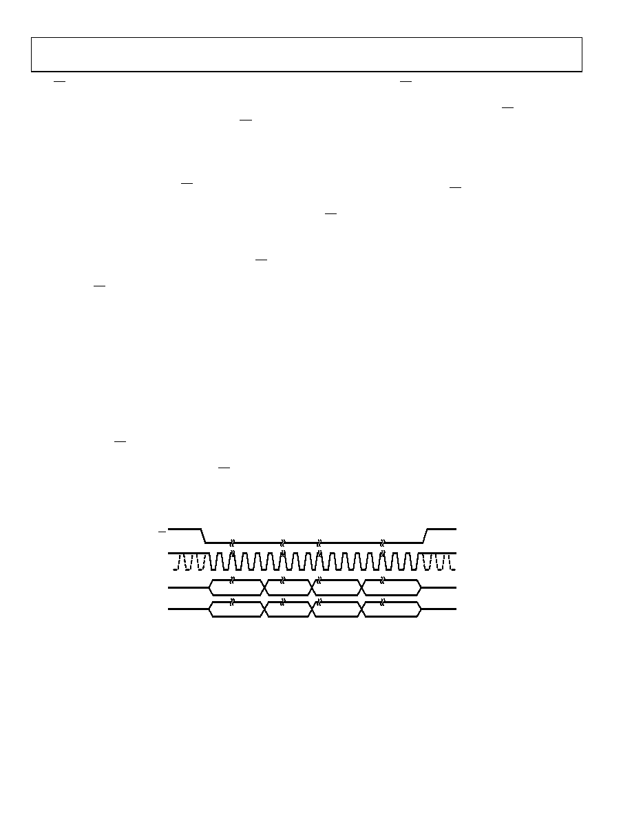
The CS falling edge takes the data output lines, DOUTA and DOUTB,
out of three-state and clocks out the MSB of the conversion
result. The rising edge of SCLK clocks all subsequent data bits
onto the serial data outputs, DOUTA and DOUTB. The CS input
can be held low for the entire serial read operation, or it can be
pulsed to frame each channel read of 16 SCLK cycles. Figure 46
shows a read of eight simultaneous conversion results using two
DOUT lines on the AD7606. In this case, a 64 SCLK transfer is used
to access data from the AD7606, and CS is held low to frame the
entire 64 SCLK cycles. Data can also be clocked out using just
one DOUT line, in which case it is recommended that DOUTA be
used to access all conversion data because the channel data is
output in ascending order. For the AD7606 to access all eight
conversion results on one DOUT line, a total of 128 SCLK cycles
is required. These 128 SCLK cycles can be framed by one CS
signal, or each group of 16 SCLK cycles can be individually
framed by the CS signal. The disadvantage of using just one
DOUT line is that the throughput rate is reduced if reading occurs
after conversion. The unused DOUT line should be left unconnected
in serial mode. For the AD7606, if DOUTB is to be used as a single
DOUT line, the channel results are output in the following order:
V5, V6, V7, V8, V1, V2, V3, and V4; however, the FRSTDATA
indicator returns low after V5 is read on DOUTB. For the AD7606-6
and the AD7606-4, if DOUTB is to be used as a single DOUT line,
the channel results are output in the following order: V4, V5, V6,
V1, V2, and V3 for the AD7606-6; and V3, V4, V1, and V2 for
the AD7606-4.
Figure 6 shows the timing diagram for reading one channel of
data, framed by the CS signal, from the AD7606/AD7606-6/
AD7606-4 in serial mode. The SCLK input signal provides the
clock source for the serial read operation. The CS goes low to
access the data from the AD7606/AD7606-6/AD7606-4.
The falling edge of CS takes the bus out of three-state and clocks
out the MSB of the 16-bit conversion result. This MSB is valid
on the first falling edge of the SCLK after the CS falling edge.
The subsequent 15 data bits are clocked out of the AD7606/
AD7606-6/AD7606-4 on the SCLK rising edge. Data is valid on
the SCLK falling edge. To access each conversion result, 16 clock
cycles must be provided to the AD7606/AD7606-6/AD7606-4.
The FRSTDATA output signal indicates when the first channel,
V1, is being read back. When the CS input is high, the FRSTDATA
output pin is in three-state. In serial mode, the falling edge of
CS takes FRSTDATA out of three-state and sets the FRSTDATA
pin high, indicating that the result from V1 is available on the
DOUTA output data line. The FRSTDATA output returns to
a logic low following the 16th SCLK falling edge. If all channels
are read on DOUTB, the FRSTDATA output does not go high when
V1 is being output on this serial data output pin. It goes high
only when V1 is available on DOUTA (and this is when V5 is
available on DOUTB for the AD7606).
READING DURING CONVERSION
Data can be read from the AD7606/AD7606-6/AD7606-4 while
BUSY is high and the conversions are in progress. This has little
effect on the performance of the converter, and it allows a faster
throughput rate to be achieved. A parallel, parallel byte, or serial
read can be performed during conversions and when oversampling
may or may not be in use. Figure 3 shows the timing diagram for
reading while BUSY is high in parallel or serial mode. Reading
during conversions allows the full throughput rate to be achieved
when using the serial interface with VDRIVE above 4.75 V.
Data can be read from the AD7606 at any time other than on
the falling edge of BUSY because this is when the output data
registers are updated with the new conversion data. Time t6, as
outlined in Table 3, should be observed in this condition.
V1
V4
V2
V3
V5
V8
V6
V7
SCLK
DOUTA
DOUTB
CS
64
08
47
9-
0
44
Figure 46. AD7606 Serial Interface with Two DOUT Lines
相关PDF资料 |
PDF描述 |
|---|---|
| MS3124E12-10SW | CONN RCPT 10POS JAM NUT W/SCKT |
| V110A8M200BG | CONVERTER MOD DC/DC 8V 200W |
| MS27473E18B30P | CONN PLUG 30POS STRAIGHT W/PINS |
| V110A8M200BF3 | CONVERTER MOD DC/DC 8V 200W |
| M83723/77R1412N | CONN PLUG 12POS STRAIGHT W/SCKT |
相关代理商/技术参数 |
参数描述 |
|---|---|
| AD7606BSTZ-6 | 功能描述:IC DAS W/ADC 16BIT 6CH 64LQFP RoHS:是 类别:集成电路 (IC) >> 数据采集 - ADCs/DAC - 专用型 系列:- 产品培训模块:Lead (SnPb) Finish for COTS Obsolescence Mitigation Program 标准包装:50 系列:- 类型:数据采集系统(DAS) 分辨率(位):16 b 采样率(每秒):21.94k 数据接口:MICROWIRE?,QSPI?,串行,SPI? 电压电源:模拟和数字 电源电压:1.8 V ~ 3.6 V 工作温度:-40°C ~ 85°C 安装类型:表面贴装 封装/外壳:40-WFQFN 裸露焊盘 供应商设备封装:40-TQFN-EP(6x6) 包装:托盘 |
| AD7606BSTZ-6RL | 功能描述:IC DAS W/ADC 16BIT 64LQFP RoHS:是 类别:集成电路 (IC) >> 数据采集 - ADCs/DAC - 专用型 系列:- 产品培训模块:Lead (SnPb) Finish for COTS Obsolescence Mitigation Program 标准包装:50 系列:- 类型:数据采集系统(DAS) 分辨率(位):16 b 采样率(每秒):21.94k 数据接口:MICROWIRE?,QSPI?,串行,SPI? 电压电源:模拟和数字 电源电压:1.8 V ~ 3.6 V 工作温度:-40°C ~ 85°C 安装类型:表面贴装 封装/外壳:40-WFQFN 裸露焊盘 供应商设备封装:40-TQFN-EP(6x6) 包装:托盘 |
| AD7606BSTZ-RL | 功能描述:IC DAS W/ADC 16BIT 64LQFP RoHS:是 类别:集成电路 (IC) >> 数据采集 - ADCs/DAC - 专用型 系列:- 产品培训模块:Lead (SnPb) Finish for COTS Obsolescence Mitigation Program 标准包装:50 系列:- 类型:数据采集系统(DAS) 分辨率(位):16 b 采样率(每秒):21.94k 数据接口:MICROWIRE?,QSPI?,串行,SPI? 电压电源:模拟和数字 电源电压:1.8 V ~ 3.6 V 工作温度:-40°C ~ 85°C 安装类型:表面贴装 封装/外壳:40-WFQFN 裸露焊盘 供应商设备封装:40-TQFN-EP(6x6) 包装:托盘 |
| AD7607 | 制造商:AD 制造商全称:Analog Devices 功能描述:8-Channel Differential DAS with 18-Bit, Bipolar, Simultaneous Sampling ADC |
| AD7607BSTZ | 功能描述:IC DAS W/ADC 14BIT 8CH 64LQFP RoHS:是 类别:集成电路 (IC) >> 数据采集 - ADCs/DAC - 专用型 系列:- 产品培训模块:Lead (SnPb) Finish for COTS Obsolescence Mitigation Program 标准包装:50 系列:- 类型:数据采集系统(DAS) 分辨率(位):16 b 采样率(每秒):21.94k 数据接口:MICROWIRE?,QSPI?,串行,SPI? 电压电源:模拟和数字 电源电压:1.8 V ~ 3.6 V 工作温度:-40°C ~ 85°C 安装类型:表面贴装 封装/外壳:40-WFQFN 裸露焊盘 供应商设备封装:40-TQFN-EP(6x6) 包装:托盘 |
发布紧急采购,3分钟左右您将得到回复。