参数资料
| 型号: | AD7641BSTZRL |
| 厂商: | Analog Devices Inc |
| 文件页数: | 14/28页 |
| 文件大小: | 0K |
| 描述: | IC ADC 18BIT 2MSPS SAR 48-LQFP |
| 产品培训模块: | ADC Applications ADC Architectures ADC DC/AC Performance |
| 标准包装: | 2,000 |
| 位数: | 18 |
| 采样率(每秒): | 2M |
| 数据接口: | 串行,并联 |
| 转换器数目: | 1 |
| 功率耗散(最大): | 92mW |
| 电压电源: | 模拟和数字 |
| 工作温度: | -40°C ~ 85°C |
| 安装类型: | 表面贴装 |
| 封装/外壳: | 48-LQFP |
| 供应商设备封装: | 48-LQFP(7x7) |
| 包装: | 带卷 (TR) |
| 输入数目和类型: | 1 个差分,双极 |
| 配用: | EVAL-AD7641CBZ-ND - BOARD EVALUATION FOR AD7641 |
第1页第2页第3页第4页第5页第6页第7页第8页第9页第10页第11页第12页第13页当前第14页第15页第16页第17页第18页第19页第20页第21页第22页第23页第24页第25页第26页第27页第28页
AD7641
Rev. 0 | Page 21 of 28
INTERFACES
DIGITAL INTERFACE
PARALLEL INTERFACE
The AD7641 has a versatile digital interface that can be set up
as either a serial or a parallel interface with the host system. The
serial interface is multiplexed on the parallel data bus. The AD7641
digital interface also accommodates 2.5 V, 3.3 V, or 5 V logic
with either OVDD at 2.5 V or 3.3 V. OVDD defines the logic
high output voltage. In most applications, the OVDD supply pin
of the AD7641 is connected to the host system interface 2.5 V
or 3.3 V digital supply. By using the D0/OB/
The AD7641 is configured to use the parallel interface for an
18-bit, 16-bit, or 8-bit bus width according to Table 7.
Master Parallel Interface
2C input pin, either
twos complement or straight binary coding can be used.
The two signals CS and RD control the interface. When at least
one of these signals is high, the interface outputs are in high
impedance. Usually, CS allows the selection of each AD7641 in
multicircuit applications and is held low in a single AD7641
design. RD is generally used to enable the conversion result on
the data bus.
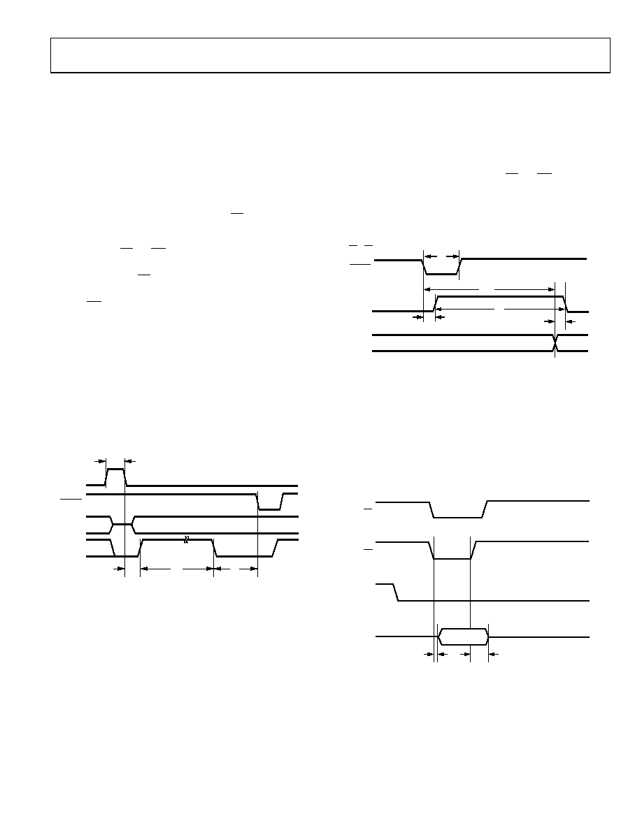
RESET
The RESET input is used to reset the AD7641 and generate a
fast initialization. A rising edge on RESET aborts the current
conversion (if any) and tristates the data bus. The falling edge of
RESET clears the data bus and engages the initialization process
indicated by pulsing BUSY high. Conversions can take place
after the falling edge of BUSY. Refer to Figure 30 for the RESET
timing details.
0
47
61
-0
31
RESET
DATA
BUSY
CNVST
t38
t39
t8
t9
Figure 30. RESET Timing
Data can be continuously read by tying CS
RD
and
low, thus
requiring minimal microprocessor connections. However, in
this mode, the data bus is always driven and cannot be used in
shared bus applications, unless the device is held in RESET.
Figure 31 details the timing for this mode.
04
761
-03
2
t1
BUSY
DATA
BUS
PREVIOUS CONVERSION DATA
NEW DATA
CNVST
CS = RD = 0
t10
t4
t11
t3
Figure 31. Master Parallel Data Timing for Reading (Continuous Read)
Slave Parallel Interface
In slave parallel reading mode, the data can be read either after
each conversion, which is during the next acquisition phase, or
during the following conversion, as shown in Figure 32 and
Figure 33, respectively. When the data is read during the
conversion, it is recommended that it is read-only during the
first half of the conversion phase. This avoids any potential
feedthrough between voltage transients on the digital interface
and the most critical analog conversion circuitry.
04
76
1-
03
3
CURRENT
CONVERSION
t13
t12
BUSY
DATA
BUS
RD
CS
Figure 32. Slave Parallel Data Timing for Reading (Read After Convert)
相关PDF资料 |
PDF描述 |
|---|---|
| AD7643BCPZ | IC ADC 18BIT DIFF W/REF 48LFCSP |
| AD7650ACPZ | IC ADC 16BIT CMOS 5V 48LFCSP |
| AD7651ACPZ | IC ADC 16BIT UNIPOLAR 48LFCSP |
| AD7652ASTZ | IC ADC 16BIT 500KSPS REF 48LQFP |
| AD7653ACPZRL | IC ADC 16BIT UNIPOLAR 48LFCSP |
相关代理商/技术参数 |
参数描述 |
|---|---|
| AD7641XST | 制造商:Analog Devices 功能描述: |
| AD7641XST-U3 | 制造商:Analog Devices 功能描述: |
| AD7643 | 制造商:AD 制造商全称:Analog Devices 功能描述:14-Bit, 1 MSPS, Differential, Programmable Input PulSAR ADC |
| AD7643BCPZ | 功能描述:IC ADC 18BIT DIFF W/REF 48LFCSP RoHS:是 类别:集成电路 (IC) >> 数据采集 - 模数转换器 系列:PulSAR® 标准包装:1 系列:- 位数:14 采样率(每秒):83k 数据接口:串行,并联 转换器数目:1 功率耗散(最大):95mW 电压电源:双 ± 工作温度:0°C ~ 70°C 安装类型:通孔 封装/外壳:28-DIP(0.600",15.24mm) 供应商设备封装:28-PDIP 包装:管件 输入数目和类型:1 个单端,双极 |
| AD7643BCPZRL | 功能描述:IC ADC 18BIT DIFF W/REF 48-LFCSP RoHS:是 类别:集成电路 (IC) >> 数据采集 - 模数转换器 系列:PulSAR® 标准包装:1 系列:- 位数:14 采样率(每秒):83k 数据接口:串行,并联 转换器数目:1 功率耗散(最大):95mW 电压电源:双 ± 工作温度:0°C ~ 70°C 安装类型:通孔 封装/外壳:28-DIP(0.600",15.24mm) 供应商设备封装:28-PDIP 包装:管件 输入数目和类型:1 个单端,双极 |
发布紧急采购,3分钟左右您将得到回复。