参数资料
| 型号: | AD7641BSTZRL |
| 厂商: | Analog Devices Inc |
| 文件页数: | 15/28页 |
| 文件大小: | 0K |
| 描述: | IC ADC 18BIT 2MSPS SAR 48-LQFP |
| 产品培训模块: | ADC Applications ADC Architectures ADC DC/AC Performance |
| 标准包装: | 2,000 |
| 位数: | 18 |
| 采样率(每秒): | 2M |
| 数据接口: | 串行,并联 |
| 转换器数目: | 1 |
| 功率耗散(最大): | 92mW |
| 电压电源: | 模拟和数字 |
| 工作温度: | -40°C ~ 85°C |
| 安装类型: | 表面贴装 |
| 封装/外壳: | 48-LQFP |
| 供应商设备封装: | 48-LQFP(7x7) |
| 包装: | 带卷 (TR) |
| 输入数目和类型: | 1 个差分,双极 |
| 配用: | EVAL-AD7641CBZ-ND - BOARD EVALUATION FOR AD7641 |
第1页第2页第3页第4页第5页第6页第7页第8页第9页第10页第11页第12页第13页第14页当前第15页第16页第17页第18页第19页第20页第21页第22页第23页第24页第25页第26页第27页第28页
AD7641
Rev. 0 | Page 22 of 28
0
45
76
1-
0
3
4
PREVIOUS
CONVERSION
t13
t12
t3
BUSY
DATA
BUS
CNVST,
RD
CS = 0
t4
t1
SERIAL INTERFACE
The AD7641 is configured to use the serial interface when
MODE[1:0] = 3. The AD7641 outputs 18 bits of data, MSB first,
on the SDOUT pin. This data is synchronized with the 18 clock
pulses provided on the SCLK pin. The output data is valid on
both the rising and falling edge of the data clock.
MASTER SERIAL INTERFACE
Internal Clock
The AD7641 is configured to generate and provide the serial
data clock SCLK when the EXT/INT pin is held low. The
AD7641 also generates a SYNC signal to indicate to the host
when the serial data is valid. The serial clock SCLK and the
SYNC signal can be inverted. Depending on the read during
convert input, RDC/SDIN, the data can be read after each
conversion or during the following conversion.
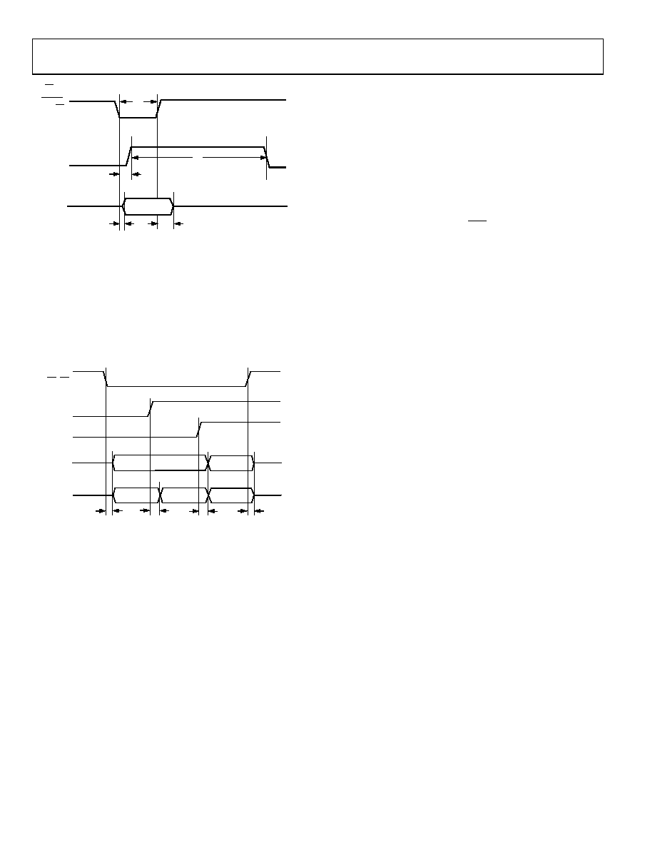
Figure 33. Slave Parallel Data Timing for Reading (Read During Convert)
16-Bit and 8-Bit Interface (Master or Slave)
In the 16-bit (MODE[1:0] = 1) and 8-bit (MODE[1:0] = 2)
interfaces, the A0/A1 pins allow a glueless interface to a 16- or
8-bit bus, as shown in
Figure 35 and
Figure 34. By connecting A0/A1 to an
address line(s), the data can be read in two words for a 16-bit
interface, or three bytes for an 8-bit interface. This interface can
be used in both master and slave parallel reading modes. Refer
to
Figure 36 show detailed timing diagrams of these two modes.
Usually, because the AD7641 is used with a fast throughput, the
master read during conversion mode is the most recommended
serial mode. In this mode, the serial clock and data toggle at
appropriate instants, minimizing potential feedthrough between
digital activity and critical conversion decisions. In this mode,
the SCLK period changes because the LSBs require more time
to settle and the SCLK is derived from the SAR conversion cycle.
Table 7 for the full details of the interface.
CS, RD
A1
D[17:2]
HI-Z
HIGH
WORD
LOW
WORD
HI-Z
t12
t13
04
76
1-
0
35
HIGH
BYTE
A0
MID
BYTE
LOW
BYTE
D[17:10]
t12
HI-Z
t12
In read after conversion mode, it should be noted that unlike
other modes, the BUSY signal returns low after the 18 data bits
are pulsed out and not at the end of the conversion phase,
resulting in a longer BUSY width. As a result, the maximum
throughput cannot be achieved in this mode.
In addition, in read after convert mode, the SCLK frequency
can be slowed down to accommodate different hosts using the
DIVSCLK[1:0] inputs. Refer to
Figure 34. 8-Bit and 16-Bit Parallel Interface
Table 4 for the SCLK timing
details when using these inputs.
相关PDF资料 |
PDF描述 |
|---|---|
| AD7643BCPZ | IC ADC 18BIT DIFF W/REF 48LFCSP |
| AD7650ACPZ | IC ADC 16BIT CMOS 5V 48LFCSP |
| AD7651ACPZ | IC ADC 16BIT UNIPOLAR 48LFCSP |
| AD7652ASTZ | IC ADC 16BIT 500KSPS REF 48LQFP |
| AD7653ACPZRL | IC ADC 16BIT UNIPOLAR 48LFCSP |
相关代理商/技术参数 |
参数描述 |
|---|---|
| AD7641XST | 制造商:Analog Devices 功能描述: |
| AD7641XST-U3 | 制造商:Analog Devices 功能描述: |
| AD7643 | 制造商:AD 制造商全称:Analog Devices 功能描述:14-Bit, 1 MSPS, Differential, Programmable Input PulSAR ADC |
| AD7643BCPZ | 功能描述:IC ADC 18BIT DIFF W/REF 48LFCSP RoHS:是 类别:集成电路 (IC) >> 数据采集 - 模数转换器 系列:PulSAR® 标准包装:1 系列:- 位数:14 采样率(每秒):83k 数据接口:串行,并联 转换器数目:1 功率耗散(最大):95mW 电压电源:双 ± 工作温度:0°C ~ 70°C 安装类型:通孔 封装/外壳:28-DIP(0.600",15.24mm) 供应商设备封装:28-PDIP 包装:管件 输入数目和类型:1 个单端,双极 |
| AD7643BCPZRL | 功能描述:IC ADC 18BIT DIFF W/REF 48-LFCSP RoHS:是 类别:集成电路 (IC) >> 数据采集 - 模数转换器 系列:PulSAR® 标准包装:1 系列:- 位数:14 采样率(每秒):83k 数据接口:串行,并联 转换器数目:1 功率耗散(最大):95mW 电压电源:双 ± 工作温度:0°C ~ 70°C 安装类型:通孔 封装/外壳:28-DIP(0.600",15.24mm) 供应商设备封装:28-PDIP 包装:管件 输入数目和类型:1 个单端,双极 |
发布紧急采购,3分钟左右您将得到回复。