参数资料
| 型号: | AD7641BSTZRL |
| 厂商: | Analog Devices Inc |
| 文件页数: | 27/28页 |
| 文件大小: | 0K |
| 描述: | IC ADC 18BIT 2MSPS SAR 48-LQFP |
| 产品培训模块: | ADC Applications ADC Architectures ADC DC/AC Performance |
| 标准包装: | 2,000 |
| 位数: | 18 |
| 采样率(每秒): | 2M |
| 数据接口: | 串行,并联 |
| 转换器数目: | 1 |
| 功率耗散(最大): | 92mW |
| 电压电源: | 模拟和数字 |
| 工作温度: | -40°C ~ 85°C |
| 安装类型: | 表面贴装 |
| 封装/外壳: | 48-LQFP |
| 供应商设备封装: | 48-LQFP(7x7) |
| 包装: | 带卷 (TR) |
| 输入数目和类型: | 1 个差分,双极 |
| 配用: | EVAL-AD7641CBZ-ND - BOARD EVALUATION FOR AD7641 |
第1页第2页第3页第4页第5页第6页第7页第8页第9页第10页第11页第12页第13页第14页第15页第16页第17页第18页第19页第20页第21页第22页第23页第24页第25页第26页当前第27页第28页
AD7641
Rev. 0 | Page 8 of 28
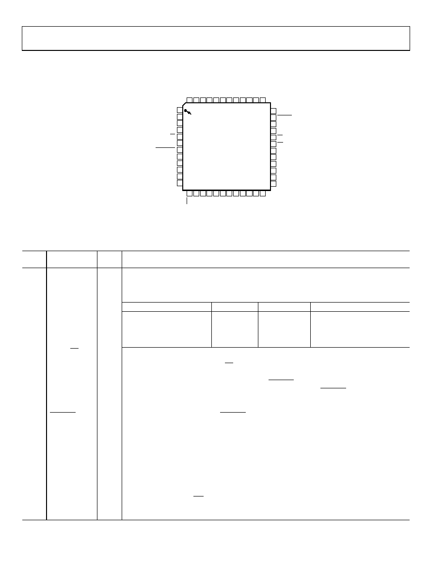
PIN CONFIGURATION AND FUNCTION DESCRIPTIONS
36
35
34
33
32
31
30
29
28
27
26
25
13 14 15 16 17 18 19 20 21 22 23 24
1
2
3
4
5
6
7
8
9
10
11
12
48 47 46 45 44
39 38 37
43 42 41 40
PIN 1
IDENTIFIER
TOP VIEW
(Not to Scale)
AGND
CNVST
PD
RESET
CS
RD
DGND
AGND
AVDD
MODE0
MODE1
D0/OB/2C
NC = NO CONNECT
D1/A0
D2/A1
D3
D4/DIVSCLK[0]
BUSY
D17
D16
D15
AD7641
D5/DIVSCLK[1]
D14
D
6/
E
X
T
/IN
T
D
7/
IN
VSYN
C
D8/
IN
V
S
CL
K
D9/
RDC/
S
D
IN
OG
N
D
OV
D
DV
DD
DG
ND
D10/
S
D
O
U
T
D1
1/
SC
LK
D12
/S
Y
NC
D13
/RDE
RRO
R
P
DBUF
P
DRE
F
RE
F
BUF
IN
TE
M
P
AV
D
IN
+
AG
ND
AG
ND
NC
IN
–
RE
F
G
ND
RE
F
WARP
04
76
1-
0
04
NORMAL
Figure 4. Pin Configuration
Table 6. Pin Function Descriptions
Pin
No.
Mnemonic
Type1
Description
1, 36,
41, 42
AGND
P
Analog Power Ground Pin.
2, 44
AVDD
P
Input Analog Power Pins. Nominally 2.5 V.
3, 4
MODE[0:1]
DI
Data Output Interface Mode Selection.
Interface MODE#
MODE1
MODE0
Description
0
18-bit interface
1
0
1
16-bit interface
2
1
0
8-bit (byte) interface
3
1
Serial interface
5
D0/OB/2C
DI/O
When MODE[1:0] = 0 (18-bit interface mode), this pin is Bit 0 of the parallel port data output bus
and the data coding is straight binary. In all other modes, this pin allows the choice of straight
binary/twos complement. When OB/2C is high, the digital output is straight binary; when low,
the MSB is inverted resulting in a twos complement output from its internal shift register.
6
WARP
DI
Conversion Mode Selection. When WARP = high and NORMAL = high, this selects wideband warp
mode with slightly improved linearity and THD. When WARP = high and NORMAL = low, this selects
warp mode. In either mode, these are the fastest modes; maximum throughput is achievable, and
a minimum conversion rate must be applied to guarantee full specified accuracy.
7
NORMAL
DI
Conversion Mode Selection. When NORMAL = low and WARP = low, this input selects normal mode
where full accuracy is maintained independent of the minimum conversion rate.
8
D1/A0
DI/O
When MODE[1:0] = 0, this pin is Bit 1 of the parallel port data output bus. In all other modes, this
input pin controls the form in which data is output as shown in Table 7.
9
D2/A1
DI/O
When MODE[1:0] = 0, this pin is Bit 2 of the parallel port data output bus.
When MODE[1:0] = 1 or 2, this input pin controls the form in which data is output as shown in Table 7.
10
D3
D0
When MODE[1:0] = 0, 1, or 2, this output is used as Bit 3 of the parallel port data output bus.
This pin is always an output, regardless of the interface mode.
11, 12
D[4:5]
DI/O
When MODE[1:0] = 0, 1, or 2, these pins are Bit 4 and Bit 5 of the parallel port data output bus.
or DIVSCLK[0:1]
When MODE[1:0] = 3 (serial mode), serial clock division selection. When using serial master read
after convert mode (EXT/INT = low, RDC/SDIN = low), these inputs can be used to slow down the
internally generated serial clock that clocks the data output. In other serial modes, these pins are
high impedance outputs.
相关PDF资料 |
PDF描述 |
|---|---|
| AD7643BCPZ | IC ADC 18BIT DIFF W/REF 48LFCSP |
| AD7650ACPZ | IC ADC 16BIT CMOS 5V 48LFCSP |
| AD7651ACPZ | IC ADC 16BIT UNIPOLAR 48LFCSP |
| AD7652ASTZ | IC ADC 16BIT 500KSPS REF 48LQFP |
| AD7653ACPZRL | IC ADC 16BIT UNIPOLAR 48LFCSP |
相关代理商/技术参数 |
参数描述 |
|---|---|
| AD7641XST | 制造商:Analog Devices 功能描述: |
| AD7641XST-U3 | 制造商:Analog Devices 功能描述: |
| AD7643 | 制造商:AD 制造商全称:Analog Devices 功能描述:14-Bit, 1 MSPS, Differential, Programmable Input PulSAR ADC |
| AD7643BCPZ | 功能描述:IC ADC 18BIT DIFF W/REF 48LFCSP RoHS:是 类别:集成电路 (IC) >> 数据采集 - 模数转换器 系列:PulSAR® 标准包装:1 系列:- 位数:14 采样率(每秒):83k 数据接口:串行,并联 转换器数目:1 功率耗散(最大):95mW 电压电源:双 ± 工作温度:0°C ~ 70°C 安装类型:通孔 封装/外壳:28-DIP(0.600",15.24mm) 供应商设备封装:28-PDIP 包装:管件 输入数目和类型:1 个单端,双极 |
| AD7643BCPZRL | 功能描述:IC ADC 18BIT DIFF W/REF 48-LFCSP RoHS:是 类别:集成电路 (IC) >> 数据采集 - 模数转换器 系列:PulSAR® 标准包装:1 系列:- 位数:14 采样率(每秒):83k 数据接口:串行,并联 转换器数目:1 功率耗散(最大):95mW 电压电源:双 ± 工作温度:0°C ~ 70°C 安装类型:通孔 封装/外壳:28-DIP(0.600",15.24mm) 供应商设备封装:28-PDIP 包装:管件 输入数目和类型:1 个单端,双极 |
发布紧急采购,3分钟左右您将得到回复。