参数资料
| 型号: | AD7641BSTZRL |
| 厂商: | Analog Devices Inc |
| 文件页数: | 24/28页 |
| 文件大小: | 0K |
| 描述: | IC ADC 18BIT 2MSPS SAR 48-LQFP |
| 产品培训模块: | ADC Applications ADC Architectures ADC DC/AC Performance |
| 标准包装: | 2,000 |
| 位数: | 18 |
| 采样率(每秒): | 2M |
| 数据接口: | 串行,并联 |
| 转换器数目: | 1 |
| 功率耗散(最大): | 92mW |
| 电压电源: | 模拟和数字 |
| 工作温度: | -40°C ~ 85°C |
| 安装类型: | 表面贴装 |
| 封装/外壳: | 48-LQFP |
| 供应商设备封装: | 48-LQFP(7x7) |
| 包装: | 带卷 (TR) |
| 输入数目和类型: | 1 个差分,双极 |
| 配用: | EVAL-AD7641CBZ-ND - BOARD EVALUATION FOR AD7641 |
第1页第2页第3页第4页第5页第6页第7页第8页第9页第10页第11页第12页第13页第14页第15页第16页第17页第18页第19页第20页第21页第22页第23页当前第24页第25页第26页第27页第28页
AD7641
Rev. 0 | Page 5 of 28
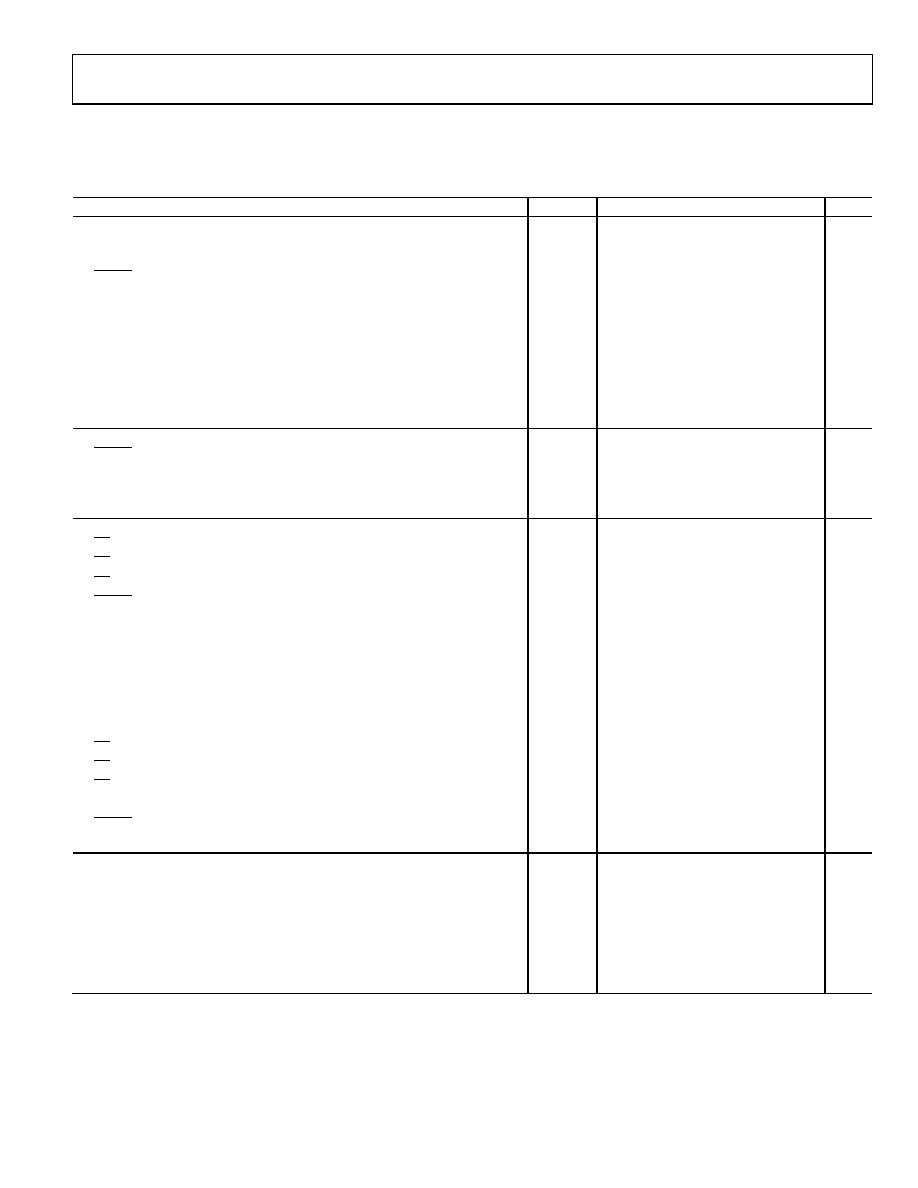
TIMING SPECIFICATIONS
AVDD = DVDD = 2.5 V; OVDD = 2.3 V to 3.6 V; VREF = 2.5 V; all specifications TMIN to TMAX, unless otherwise noted.
Table 3.
Parameter
Symbol
Min
Typ
Max
Unit
Convert Pulse Width
t1
15
701
ns
t2
500/667
ns
CNVST Low to BUSY High Delay
t3
23
ns
BUSY High All Modes (Except Master Serial Read After Convert)
t4
385/520
ns
Aperture Delay
t5
1
ns
End of Conversion to BUSY Low Delay
t6
10
ns
Conversion Time (Warp Mode/Normal Mode)
t7
385/520
ns
Acquisition Time (Warp Mode/Normal Mode)
t8
115
ns
RESET Pulse Width
t9
15
ns
RESET Low to BUSY High Delay4
t38
10
ns
BUSY High Time from RESET Low4
t39
600
ns
CNVST Low to Data Valid Delay (Warp Mode/Normal Mode)
t10
385/520
ns
Data Valid to BUSY Low Delay
t11
2
ns
Bus Access Request to Data Valid
t12
20
ns
Bus Relinquish Time
t13
2
15
ns
CS Low to SYNC Valid Delay
t14
10
ns
CS Low to Internal SCLK Valid Delay5
t15
10
ns
CS Low to SDOUT Delay
t16
10
ns
CNVST Low to SYNC Delay (Warp Mode/Normal Mode)
t17
14/137
ns
SYNC Asserted to SCLK First Edge Delay
t18
0.5
ns
Internal SCLK Period6
t19
8
14
ns
Internal SCLK High6
t20
2
ns
Internal SCLK Low6
t21
3
ns
SDOUT Valid Setup Time6
t22
1
ns
SDOUT Valid Hold Time6
t23
0
ns
SCLK Last Edge to SYNC Delay6
t24
0
ns
CS High to SYNC HI-Z
t25
10
ns
CS High to Internal SCLK HI-Z
t26
10
ns
CS High to SDOUT HI-Z
t27
10
ns
BUSY High in Master Serial Read After Convert6
t28
See Table 4
ns
CNVST Low to SYNC Asserted Delay (All Modes)
t29
383/500
ns
SYNC Deasserted to BUSY Low Delay
t30
13
ns
External SCLK Setup Time
t31
5
ns
External SCLK Active Edge to SDOUT Delay
t32
1
8
ns
SDIN Setup Time
t33
5
ns
SDIN Hold Time
t34
5
ns
External SCLK Period
t35
12.5
ns
External SCLK High
t36
5
ns
External SCLK Low
t37
5
ns
2 All timings for wideband warp mode are the same as warp mode.
3 In warp mode only, the maximum time between conversions is 1 ms; otherwise, there is no required maximum time.
5 In serial interface modes, the SYNC, SCLK, and SDOUT timings are defined with a maximum load CL of 10 pF; otherwise, the load is 60 pF maximum.
6 In serial master read during convert mode. See Table 4 for serial master read after convert mode timing specifications.
相关PDF资料 |
PDF描述 |
|---|---|
| AD7643BCPZ | IC ADC 18BIT DIFF W/REF 48LFCSP |
| AD7650ACPZ | IC ADC 16BIT CMOS 5V 48LFCSP |
| AD7651ACPZ | IC ADC 16BIT UNIPOLAR 48LFCSP |
| AD7652ASTZ | IC ADC 16BIT 500KSPS REF 48LQFP |
| AD7653ACPZRL | IC ADC 16BIT UNIPOLAR 48LFCSP |
相关代理商/技术参数 |
参数描述 |
|---|---|
| AD7641XST | 制造商:Analog Devices 功能描述: |
| AD7641XST-U3 | 制造商:Analog Devices 功能描述: |
| AD7643 | 制造商:AD 制造商全称:Analog Devices 功能描述:14-Bit, 1 MSPS, Differential, Programmable Input PulSAR ADC |
| AD7643BCPZ | 功能描述:IC ADC 18BIT DIFF W/REF 48LFCSP RoHS:是 类别:集成电路 (IC) >> 数据采集 - 模数转换器 系列:PulSAR® 标准包装:1 系列:- 位数:14 采样率(每秒):83k 数据接口:串行,并联 转换器数目:1 功率耗散(最大):95mW 电压电源:双 ± 工作温度:0°C ~ 70°C 安装类型:通孔 封装/外壳:28-DIP(0.600",15.24mm) 供应商设备封装:28-PDIP 包装:管件 输入数目和类型:1 个单端,双极 |
| AD7643BCPZRL | 功能描述:IC ADC 18BIT DIFF W/REF 48-LFCSP RoHS:是 类别:集成电路 (IC) >> 数据采集 - 模数转换器 系列:PulSAR® 标准包装:1 系列:- 位数:14 采样率(每秒):83k 数据接口:串行,并联 转换器数目:1 功率耗散(最大):95mW 电压电源:双 ± 工作温度:0°C ~ 70°C 安装类型:通孔 封装/外壳:28-DIP(0.600",15.24mm) 供应商设备封装:28-PDIP 包装:管件 输入数目和类型:1 个单端,双极 |
发布紧急采购,3分钟左右您将得到回复。