- 您现在的位置:买卖IC网 > PDF目录10530 > AD7664ACPZ (Analog Devices Inc)IC ADC 16BIT UNIPOLAR 48-LFCSP PDF资料下载
参数资料
| 型号: | AD7664ACPZ |
| 厂商: | Analog Devices Inc |
| 文件页数: | 5/24页 |
| 文件大小: | 0K |
| 描述: | IC ADC 16BIT UNIPOLAR 48-LFCSP |
| 标准包装: | 13 |
| 系列: | PulSAR® |
| 位数: | 16 |
| 采样率(每秒): | 570k |
| 数据接口: | 串行,并联 |
| 转换器数目: | 1 |
| 功率耗散(最大): | 115mW |
| 电压电源: | 模拟和数字 |
| 工作温度: | -40°C ~ 85°C |
| 安装类型: | 表面贴装 |
| 封装/外壳: | 48-VFQFN 裸露焊盘,CSP |
| 供应商设备封装: | 48-LFCSP-VQ(7x7) |
| 包装: | 托盘 |
| 输入数目和类型: | 2 个伪差分,单极 |
| 配用: | EVAL-AD7664CBZ-ND - BOARD EVALUATION FOR AD7664 |
REV. E
AD7664
–13–
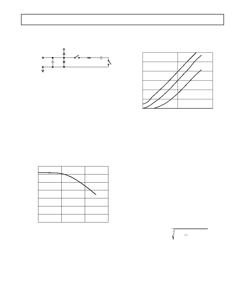
Analog Input
Figure 6 shows an equivalent circuit of the input structure of
the AD7664.
C2
R1
D1
D2
C1
IN
OR INGND
AGND
AVDD
Figure 6. Equivalent Analog Input Circuit
The two diodes D1 and D2 provide ESD protection for the
analog inputs IN and INGND. Care must be taken to ensure
that the analog input signal never exceeds the supply rails by more
than 0.3 V. This will cause these diodes to become forward-
biased and start conducting current. These diodes can handle
a forward-biased current of 100 mA maximum. For instance,
these conditions could eventually occur when the input buffer’s
(U1) supplies are different from AVDD. In such cases, an input
buffer with a short circuit current limitation can be used to
protect the part.
This analog input structure allows the sampling of the differen-
tial signal between IN and INGND. Unlike other converters,
the INGND input is sampled at the same time as the IN input.
By using this differential input, small signals common to both
inputs are rejected, as shown in Figure 7, which represents the
typical CMRR over frequency. For instance, by using INGND
to sense a remote signal ground, difference of ground potentials
between the sensor and the local ADC ground are eliminated.
70
1k
CMRR
–
dB
FREQUENCY – Hz
1M
50
30
0
100k
60
40
20
10
10k
Figure 7. Analog Input CMRR vs. Frequency
During the acquisition phase, the impedance of the analog input
IN can be modeled as a parallel combination of capacitor C1
and the network formed by the series connection of R1 and C2.
Capacitor C1 is primarily the pin capacitance. The resistor R1 is
typically 140
and is a lumped component made up of some
serial resistors and the on resistance of the switches. The capacitor
C2 is typically 60 pF and is mainly the ADC sampling capacitor.
During the conversion phase, where the switches are opened, the input
impedance is limited to C1. The R1, C2 makes a one-pole low-pass
filter that reduces the undesirable aliasing effect and limits the noise.
When the source impedance of the driving circuit is low, the
AD7664 can be driven directly. Large source impedances will
significantly affect the ac performances, especially the total
harmonic distortion (THD). The maximum source impedance
depends on the amount of THD that can be tolerated. The
THD degrades in function of the source impedance and the
maximum input frequency as shown in Figure 8.
10
THD
–
dB
FREQUENCY – kHz
100
–85
–90
–95
–100
–70
–80
1000
–75
R = 11
R = 100
R = 50
Figure 8. THD vs. Analog Input Frequency and
Source Resistance
Driver Amplifier Choice
Although the AD7664 is easy to drive, the driver amplifier needs
to meet at least the following requirements:
The driver amplifier and the AD7664 analog input circuit
must be able, together, to settle for a full-scale step of the
capacitor array at a 16-bit level (0.0015%). In the amplifier’s
data sheet, the settling at 0.1% to 0.01% is more commonly
specified. It could significantly differ from the settling time at
16-bit level and it should, therefore, be verified prior to the
driver selection. The tiny op amp AD8021, which combines
ultralow noise and a high gain bandwidth, meets this settling
time requirement even when used with high gain up to 13.
The noise generated by the driver amplifier needs to be kept as
low as possible in order to preserve the SNR and transition
noise performance of the AD7664. The noise coming from
the driver is filtered by the AD7664 analog input circuit one-
pole low-pass filter made by R1 and C2 or the external filter, if
any is used. The SNR degradation due to the amplifier is:
SNR
fNe
LOSS
–3dB
N
=
+
()
20
28
784
2
log
π
where:
f–3 dB is the –3 dB input bandwidth in MHz of the AD7664
(18 MHz) or the cutoff frequency of the input filter, if
any used.
N
is the noise gain of the amplifier (1, if in buffer
configuration).
eN
is the equivalent input noise voltage of the op amp in
nV/
√Hz.
相关PDF资料 |
PDF描述 |
|---|---|
| MS3120E12-10P | CONN RECEPT 10POS W/PINS CRIMP |
| 97-3108B-18-12P | CONN PLUG RT ANG 6POS W/PINS |
| LTC2223CUK#PBF | IC ADC 12BIT 80MSPS SAMPLE 48QFN |
| MS3101A16S-5P | CONN RCPT 3POS FREE HNG W/PINS |
| LTC2291IUP#PBF | IC ADC DUAL 12BIT 25MSPS 64QFN |
相关代理商/技术参数 |
参数描述 |
|---|---|
| AD7664ACPZRL | 制造商:Analog Devices 功能描述:ADC Single SAR 570ksps 16-bit Parallel/Serial 48-Pin LFCSP EP T/R 制造商:Analog Devices 功能描述:ADC SGL SAR 570KSPS 16BIT PARALLEL/SERL 48LFCSP EP - Tape and Reel |
| AD7664AST | 制造商:Analog Devices 功能描述:ADC Single SAR 570ksps 16-bit Parallel/Serial 48-Pin LQFP 制造商:Rochester Electronics LLC 功能描述:16-BIT, 500KSPS CMOS ADC - Tape and Reel 制造商:Analog Devices 功能描述:IC 16-BIT ADC |
| AD7664ASTRL | 制造商:Analog Devices 功能描述:ADC Single SAR 570ksps 16-bit Parallel/Serial 48-Pin LQFP T/R |
| AD7664ASTZ | 功能描述:IC ADC 16BIT UNIPOLAR 48-LQFP RoHS:是 类别:集成电路 (IC) >> 数据采集 - 模数转换器 系列:PulSAR® 标准包装:1 系列:microPOWER™ 位数:8 采样率(每秒):1M 数据接口:串行,SPI? 转换器数目:1 功率耗散(最大):- 电压电源:模拟和数字 工作温度:-40°C ~ 125°C 安装类型:表面贴装 封装/外壳:24-VFQFN 裸露焊盘 供应商设备封装:24-VQFN 裸露焊盘(4x4) 包装:Digi-Reel® 输入数目和类型:8 个单端,单极 产品目录页面:892 (CN2011-ZH PDF) 其它名称:296-25851-6 |
| AD7664ASTZRL | 功能描述:IC ADC 16BIT UNIPOLAR 48LQFP RoHS:是 类别:集成电路 (IC) >> 数据采集 - 模数转换器 系列:PulSAR® 标准包装:1 系列:- 位数:14 采样率(每秒):83k 数据接口:串行,并联 转换器数目:1 功率耗散(最大):95mW 电压电源:双 ± 工作温度:0°C ~ 70°C 安装类型:通孔 封装/外壳:28-DIP(0.600",15.24mm) 供应商设备封装:28-PDIP 包装:管件 输入数目和类型:1 个单端,双极 |
发布紧急采购,3分钟左右您将得到回复。