- 您现在的位置:买卖IC网 > PDF目录10530 > AD7664ACPZ (Analog Devices Inc)IC ADC 16BIT UNIPOLAR 48-LFCSP PDF资料下载
参数资料
| 型号: | AD7664ACPZ |
| 厂商: | Analog Devices Inc |
| 文件页数: | 9/24页 |
| 文件大小: | 0K |
| 描述: | IC ADC 16BIT UNIPOLAR 48-LFCSP |
| 标准包装: | 13 |
| 系列: | PulSAR® |
| 位数: | 16 |
| 采样率(每秒): | 570k |
| 数据接口: | 串行,并联 |
| 转换器数目: | 1 |
| 功率耗散(最大): | 115mW |
| 电压电源: | 模拟和数字 |
| 工作温度: | -40°C ~ 85°C |
| 安装类型: | 表面贴装 |
| 封装/外壳: | 48-VFQFN 裸露焊盘,CSP |
| 供应商设备封装: | 48-LFCSP-VQ(7x7) |
| 包装: | 托盘 |
| 输入数目和类型: | 2 个伪差分,单极 |
| 配用: | EVAL-AD7664CBZ-ND - BOARD EVALUATION FOR AD7664 |
REV. E
AD7664
–17–
Because the AD7664 is used with a fast throughput, the Mas-
ter Read During Conversion Mode is the most often recom-
mended Serial Mode, when it can be used. In this mode, the
serial clock and data toggle at appropriate instants that mini-
mize potential feedthrough between digital activity and the
critical conversion decisions.
In Read-after-Conversion Mode, it should be noted that, unlike
in other modes, the signal BUSY returns LOW after the 16 data
bits are pulsed out and not at the end of the conversion phase,
which results in a longer BUSY width.
SLAVE SERIAL INTERFACE
External Clock
The AD7664 is configured to accept an externally supplied
serial data clock on the SCLK pin when the EXT/
INT pin is
held HIGH. In this mode, several methods can be used to read
the data. The external serial clock is gated by
CS. When CS and
RD are both LOW, the data can be read after each conversion
or during the following conversion. The external clock can be
either a continuous or discontinuous clock. A discontinuous
clock can be either normally HIGH or normally LOW, when
inactive. Figures 18 and 20 show the detailed timing diagrams of
these methods.
While the AD7664 is performing a bit decision, it is important
that voltage transients not occur on digital input/output pins or
degradation of the conversion result could occur. This is par-
ticularly important during the second half of the conversion
phase, because the AD7664 provides error correction circuitry
that can correct for an improper bit decision made during the
first half of the conversion phase. For this reason, it is recom-
mended that when an external clock is being provided, it is a
discontinuous clock that is toggling only when BUSY is LOW
or, more importantly, that it does not transition during the latter
half of BUSY HIGH.
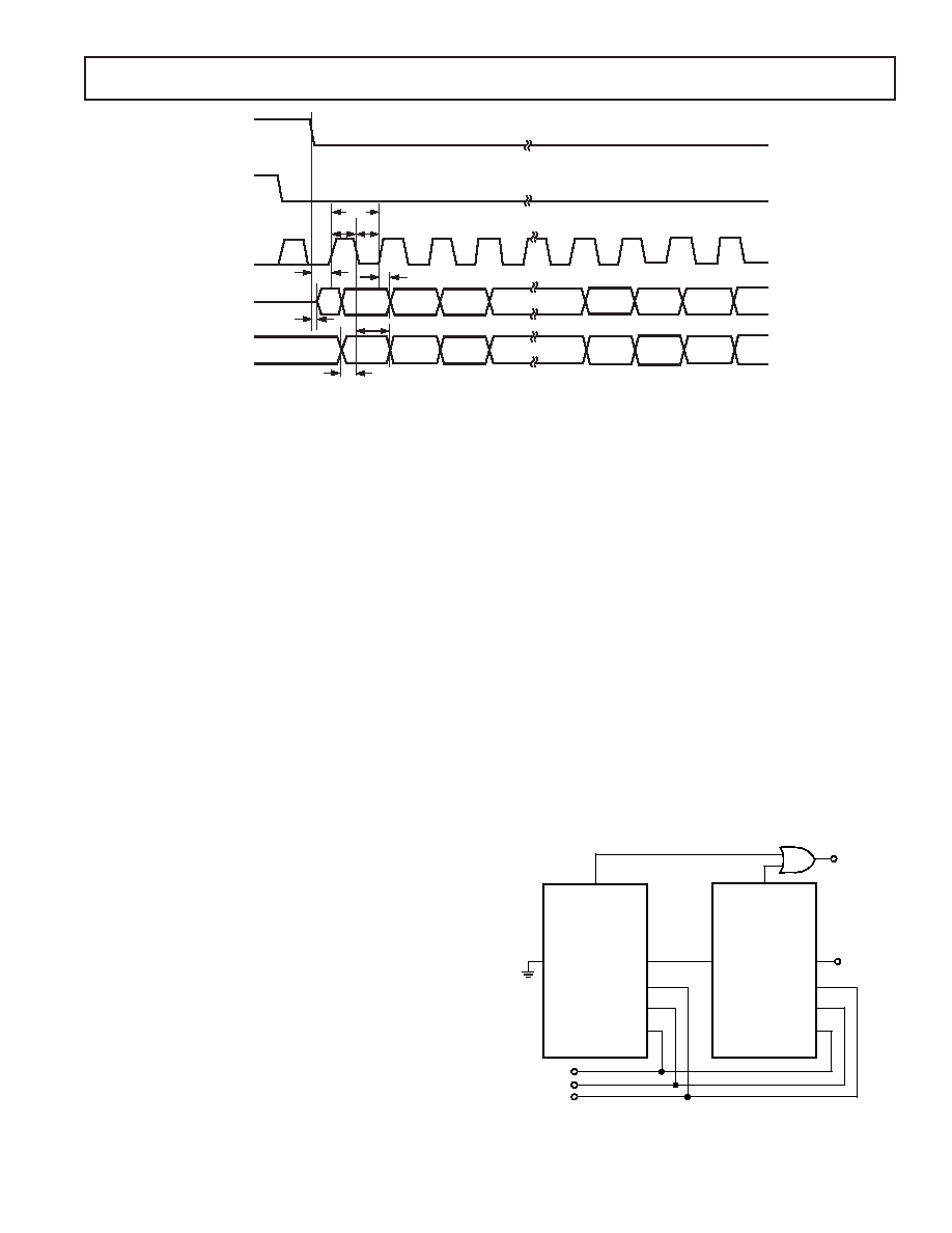
External Discontinuous Clock Data Read after Conversion
Though the maximum throughput cannot be achieved using this
mode, it is the most often recommended of the serial Slave
Modes. Figure 18 shows the detailed timing diagrams of this
method. After a conversion is complete, indicated by BUSY
returning LOW, the result of this conversion can be read
while both
CS and RD are LOW. The data is shifted out,
MSB first, with 16 clock pulses and is valid on both the rising
and falling edge of the clock.
Among the advantages of this method, the conversion perfor-
mance is not degraded, because there are no voltage tran-
sients on the digital interface during the conversion process.
Another advantage is the ability to read the data at any speed up to
40 MHz, which accommodates both slow digital host interface
and the fastest serial reading.
Finally, in this mode only, the AD7664 provides a daisy-chain
feature using the RDC/SDIN input pin for cascading multiple
converters together. This feature is useful for reducing component
count and wiring connections when desired as, for instance, in
isolated multiconverter applications.
An example of the concatenation of two devices is shown in
Figure 19. Simultaneous sampling is possible by using a com-
mon
CNVST signal. It should be noted that the RDC/SDIN
input is latched on the edge of SCLK opposite to the one used
to shift out the data on SDOUT. Therefore, the MSB of the
upstream converter just follows the LSB of the downstream
converter on the next SCLK cycle.
CNVST
CS
SCLK
SDOUT
RDC/SDIN
BUSY
DATA
OUT
AD7664
#1
(DOWNSTREAM)
BUSY
OUT
CNVST
CS
SCLK
AD7664
#2
(UPSTREAM)
RDC/SDIN
SDOUT
SCLK IN
CS IN
CNVST IN
Figure 19. Two AD7664s in a Daisy-Chain Configuration
SCLK
SDOUT
D15
D14
D1
D0
D13
X15
X14
X13
X1
X0
Y15
Y14
CS
BUSY
SDIN
EXT/
INT = 1
INVSCLK = 0
t35
t36 t37
t31
t32
t16
t33
X15
X14
X
12
3
14
15
1617
18
RD = 0
t34
Figure 18. Slave Serial Data Timing for Reading (Read after Convert)
相关PDF资料 |
PDF描述 |
|---|---|
| MS3120E12-10P | CONN RECEPT 10POS W/PINS CRIMP |
| 97-3108B-18-12P | CONN PLUG RT ANG 6POS W/PINS |
| LTC2223CUK#PBF | IC ADC 12BIT 80MSPS SAMPLE 48QFN |
| MS3101A16S-5P | CONN RCPT 3POS FREE HNG W/PINS |
| LTC2291IUP#PBF | IC ADC DUAL 12BIT 25MSPS 64QFN |
相关代理商/技术参数 |
参数描述 |
|---|---|
| AD7664ACPZRL | 制造商:Analog Devices 功能描述:ADC Single SAR 570ksps 16-bit Parallel/Serial 48-Pin LFCSP EP T/R 制造商:Analog Devices 功能描述:ADC SGL SAR 570KSPS 16BIT PARALLEL/SERL 48LFCSP EP - Tape and Reel |
| AD7664AST | 制造商:Analog Devices 功能描述:ADC Single SAR 570ksps 16-bit Parallel/Serial 48-Pin LQFP 制造商:Rochester Electronics LLC 功能描述:16-BIT, 500KSPS CMOS ADC - Tape and Reel 制造商:Analog Devices 功能描述:IC 16-BIT ADC |
| AD7664ASTRL | 制造商:Analog Devices 功能描述:ADC Single SAR 570ksps 16-bit Parallel/Serial 48-Pin LQFP T/R |
| AD7664ASTZ | 功能描述:IC ADC 16BIT UNIPOLAR 48-LQFP RoHS:是 类别:集成电路 (IC) >> 数据采集 - 模数转换器 系列:PulSAR® 标准包装:1 系列:microPOWER™ 位数:8 采样率(每秒):1M 数据接口:串行,SPI? 转换器数目:1 功率耗散(最大):- 电压电源:模拟和数字 工作温度:-40°C ~ 125°C 安装类型:表面贴装 封装/外壳:24-VFQFN 裸露焊盘 供应商设备封装:24-VQFN 裸露焊盘(4x4) 包装:Digi-Reel® 输入数目和类型:8 个单端,单极 产品目录页面:892 (CN2011-ZH PDF) 其它名称:296-25851-6 |
| AD7664ASTZRL | 功能描述:IC ADC 16BIT UNIPOLAR 48LQFP RoHS:是 类别:集成电路 (IC) >> 数据采集 - 模数转换器 系列:PulSAR® 标准包装:1 系列:- 位数:14 采样率(每秒):83k 数据接口:串行,并联 转换器数目:1 功率耗散(最大):95mW 电压电源:双 ± 工作温度:0°C ~ 70°C 安装类型:通孔 封装/外壳:28-DIP(0.600",15.24mm) 供应商设备封装:28-PDIP 包装:管件 输入数目和类型:1 个单端,双极 |
发布紧急采购,3分钟左右您将得到回复。