- 您现在的位置:买卖IC网 > PDF目录10674 > AD7682BCPZ (Analog Devices Inc)IC ADC 16BIT 4CH 250KSPS 20LFCSP PDF资料下载
参数资料
| 型号: | AD7682BCPZ |
| 厂商: | Analog Devices Inc |
| 文件页数: | 14/32页 |
| 文件大小: | 0K |
| 描述: | IC ADC 16BIT 4CH 250KSPS 20LFCSP |
| 产品培训模块: | Power Line Monitoring |
| 产品变化通告: | Startup Circuitry Design Improvement Change 15/April/2009 |
| 标准包装: | 1 |
| 系列: | PulSAR® |
| 位数: | 16 |
| 采样率(每秒): | 250k |
| 数据接口: | DSP,MICROWIRE?,QSPI?,串行,SPI? |
| 转换器数目: | 1 |
| 功率耗散(最大): | 21mW |
| 电压电源: | 模拟和数字 |
| 工作温度: | -40°C ~ 85°C |
| 安装类型: | 表面贴装 |
| 封装/外壳: | 20-VFQFN 裸露焊盘,CSP |
| 供应商设备封装: | 20-LFCSP-VQ |
| 包装: | 托盘 |
| 输入数目和类型: | 8 个单端,单极;4 个差分,双极;4 个伪差分,双极 |
| 产品目录页面: | 778 (CN2011-ZH PDF) |
第1页第2页第3页第4页第5页第6页第7页第8页第9页第10页第11页第12页第13页当前第14页第15页第16页第17页第18页第19页第20页第21页第22页第23页第24页第25页第26页第27页第28页第29页第30页第31页第32页
Data Sheet
AD7682/AD7689
Rev. D | Page 21 of 32
DRIVER AMPLIFIER CHOICE
amplifier must meet the following requirements:
The noise generated by the driver amplifier must be kept as
low as possible to preserve the SNR and transition noise
AD7689have a noise much lower than most of the other
16-bit ADCs and, therefore, can be driven by a noisier
amplifier to meet a given system noise specification. The
analog input circuit low-pass filter made by RIN and CIN or
by an external filter, if one is used. Because the typical noise
SNR degradation due to the amplifier is
+
=
2
)
(
2
π
35
log
20
N
3dB
LOSS
Ne
f
SNR
where:
AD7689 (1.7 MHz in full BW or 425 kHz in BW) or the
cutoff frequency of an input filter, if one is used.
N is the noise gain of the amplifier (for example, 1 in buffer
configuration).
eN is the equivalent input noise voltage of the op amp, in
nV/√Hz.
For ac applications, the driver should have a THD perfor-
For multichannel, multiplexed applications on each input
analog input circuit must settle a full-scale step onto the
capacitor array at a 16-bit level (0.0015%). In amplifier data
sheets, settling at 0.1% to 0.01% is more commonly
specified. This may differ significantly from the settling
time at a 16-bit level and should be verified prior to driver
selection.
Table 9. Recommended Driver Amplifiers
Amplifier
Typical Application
Very low noise, small, and low power
5 V single supply, low noise
Very low noise and high frequency
Low noise and high frequency
Low power, low noise, and low frequency
5 V single supply, low power
VOLTAGE REFERENCE OUTPUT/INPUT
ature drift internal voltage reference, an external reference, or an
external buffered reference.
lent performance and can be used in almost all applications.
There are six possible choices of voltage reference schemes
briefly described in Table 10, with more details in each of the
following sections.
Internal Reference/Temperature Sensor
The precision internal reference, suitable for most applications,
can be set for either a 2.5 V or a 4.096 V output, as detailed in
Table 10. With the internal reference enabled, the band gap
voltage is also present on the REFIN pin, which requires an
external 0.1 μF capacitor. Because the current output of REFIN
is limited, it can be used as a source if followed by a suitable
buffer, such as the AD8605. Note that the voltage of REFIN
changes depending on the 2.5 V or 4.096 V internal reference.
Enabling the reference also enables the internal temperature sensor,
and is thus useful for performing a system calibration. For
applications requiring the use of the temperature sensor, the
internal reference must be active (internal buffer can be disabled in
this case). Note that, when using the temperature sensor, the output
The internal reference is temperature-compensated to within
10 mV. The reference is trimmed to provide a typical drift of
±10 ppm/°C.
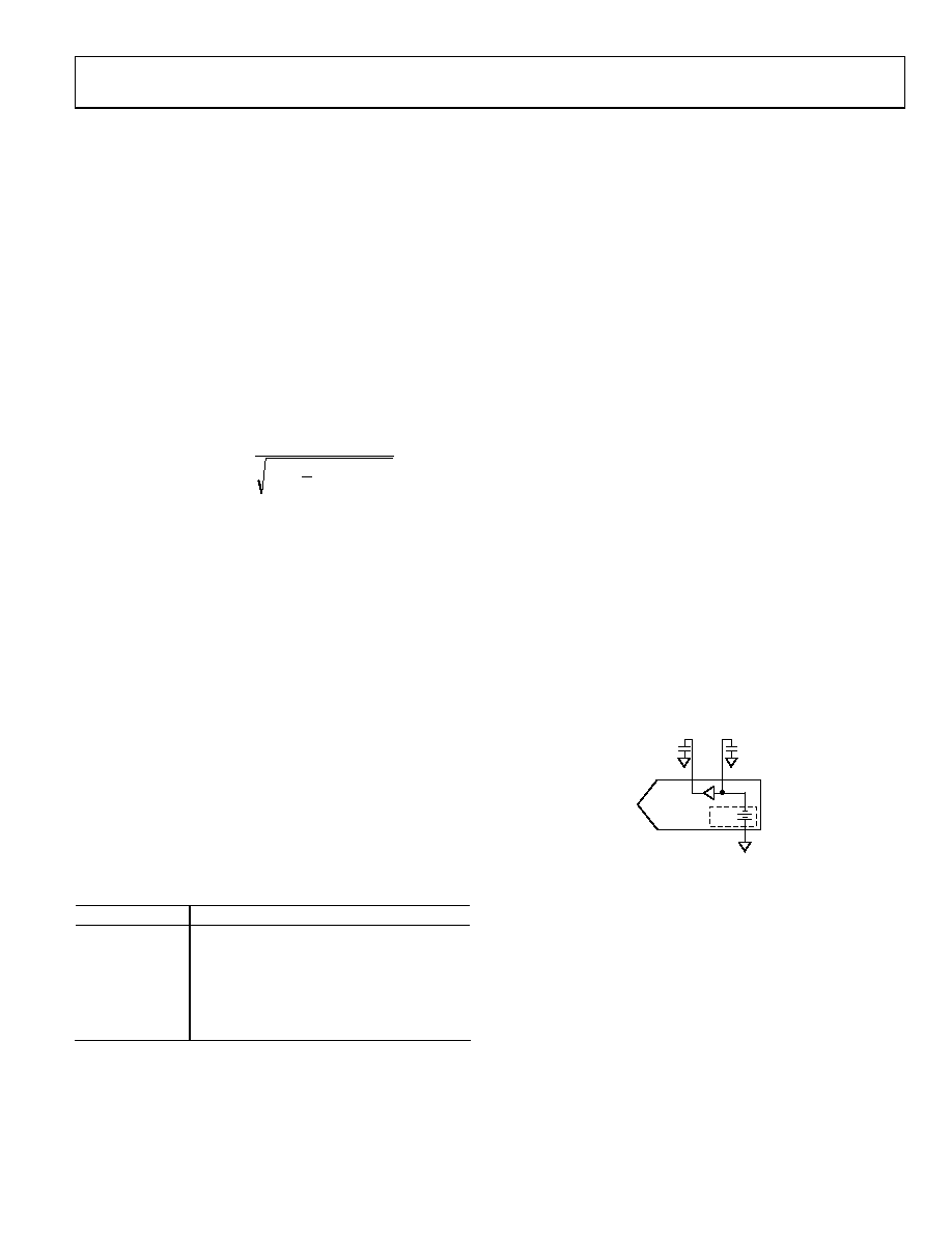
a 2.5 V or 4.096 V internal reference.
REF
GND
TEMP
AD7682/
AD7689
10F
100nF
REFIN
0
735
3-
0
49
Figure 31. 2.5 V or 4.096 V Internal Reference Connection
相关PDF资料 |
PDF描述 |
|---|---|
| AD7794BRUZ | IC ADC 24BIT SIG-DEL 6CH 24TSSOP |
| AD7689ACPZ | IC ADC 16BIT 250KSPS 8CH 20LFCSP |
| LTC1598CG#PBF | IC A/D CONV 12BIT SRL 8CH 24SSOP |
| KA339A | IC COMPARATOR QUAD 14-DIP |
| KA339 | IC COMPARATOR QUAD 14-DIP |
相关代理商/技术参数 |
参数描述 |
|---|---|
| AD7682BCPZRL7 | 功能描述:IC ADC 16BIT 4CH 250KSPS 20LFCSP RoHS:是 类别:集成电路 (IC) >> 数据采集 - 模数转换器 系列:PulSAR® 标准包装:1,000 系列:- 位数:16 采样率(每秒):45k 数据接口:串行 转换器数目:2 功率耗散(最大):315mW 电压电源:模拟和数字 工作温度:0°C ~ 70°C 安装类型:表面贴装 封装/外壳:28-SOIC(0.295",7.50mm 宽) 供应商设备封装:28-SOIC W 包装:带卷 (TR) 输入数目和类型:2 个单端,单极 |
| AD7683 | 制造商:AD 制造商全称:Analog Devices 功能描述:16-Bit, 100 kSPS PulSAR ADC in MSOP/QFN |
| AD7683ACPZRL | 功能描述:IC ADC 16BIT SRL 100KSPS 8LFCSP RoHS:是 类别:集成电路 (IC) >> 数据采集 - 模数转换器 系列:PulSAR® 标准包装:1,000 系列:- 位数:16 采样率(每秒):45k 数据接口:串行 转换器数目:2 功率耗散(最大):315mW 电压电源:模拟和数字 工作温度:0°C ~ 70°C 安装类型:表面贴装 封装/外壳:28-SOIC(0.295",7.50mm 宽) 供应商设备封装:28-SOIC W 包装:带卷 (TR) 输入数目和类型:2 个单端,单极 |
| AD7683ACPZRL7 | 功能描述:IC ADC 16BIT 100KSPS 8LFCSP RoHS:是 类别:集成电路 (IC) >> 数据采集 - 模数转换器 系列:PulSAR® 标准包装:1,000 系列:- 位数:16 采样率(每秒):45k 数据接口:串行 转换器数目:2 功率耗散(最大):315mW 电压电源:模拟和数字 工作温度:0°C ~ 70°C 安装类型:表面贴装 封装/外壳:28-SOIC(0.295",7.50mm 宽) 供应商设备封装:28-SOIC W 包装:带卷 (TR) 输入数目和类型:2 个单端,单极 |
| AD7683ARM | 制造商:Analog Devices 功能描述:ADC Single SAR 100ksps 16-bit Serial 8-Pin MSOP Tube |
发布紧急采购,3分钟左右您将得到回复。