- 您现在的位置:买卖IC网 > PDF目录10674 > AD7682BCPZ (Analog Devices Inc)IC ADC 16BIT 4CH 250KSPS 20LFCSP PDF资料下载
参数资料
| 型号: | AD7682BCPZ |
| 厂商: | Analog Devices Inc |
| 文件页数: | 21/32页 |
| 文件大小: | 0K |
| 描述: | IC ADC 16BIT 4CH 250KSPS 20LFCSP |
| 产品培训模块: | Power Line Monitoring |
| 产品变化通告: | Startup Circuitry Design Improvement Change 15/April/2009 |
| 标准包装: | 1 |
| 系列: | PulSAR® |
| 位数: | 16 |
| 采样率(每秒): | 250k |
| 数据接口: | DSP,MICROWIRE?,QSPI?,串行,SPI? |
| 转换器数目: | 1 |
| 功率耗散(最大): | 21mW |
| 电压电源: | 模拟和数字 |
| 工作温度: | -40°C ~ 85°C |
| 安装类型: | 表面贴装 |
| 封装/外壳: | 20-VFQFN 裸露焊盘,CSP |
| 供应商设备封装: | 20-LFCSP-VQ |
| 包装: | 托盘 |
| 输入数目和类型: | 8 个单端,单极;4 个差分,双极;4 个伪差分,双极 |
| 产品目录页面: | 778 (CN2011-ZH PDF) |
第1页第2页第3页第4页第5页第6页第7页第8页第9页第10页第11页第12页第13页第14页第15页第16页第17页第18页第19页第20页当前第21页第22页第23页第24页第25页第26页第27页第28页第29页第30页第31页第32页
AD7682/AD7689
Data Sheet
Rev. D | Page 28 of 32
CHANNEL SEQUENCER
scanning channels in a repeated fashion. Channels are scanned
as singles or pairs, with or without the temperature sensor, after
the last channel is sequenced.
The sequencer starts with IN0 and finishes with IN[7:0] set in
CFG[9:7]. For paired channels, the channels are paired depend-
ing on the last channel set in CFG[9:7]. Note that in sequencer
mode, the channels are always paired with the positive input on
the even channels (IN0, IN2, IN4, IN6), and with the negative
input on the odd channels (IN1, IN3, IN5, IN7). For example,
setting CFG[9:7] = 110 or 111 scans all pairs with the positive
inputs dedicated to IN0, IN2, IN4, and IN6.
CFG[2:1] are used to enable the sequencer. After the CFG
register is updated, DIN must be held low while reading data
out for Bit 13, or the CFG register begins updating again.
Note that while operating in a sequence, some bits of the CFG
register can be changed. However, if changing CFG[11] (paired
or single channel) or CFG[9:7] (last channel in sequence), the
sequence reinitializes and converts IN0 (or IN0/IN1 pairs) after
the CFG register is updated.
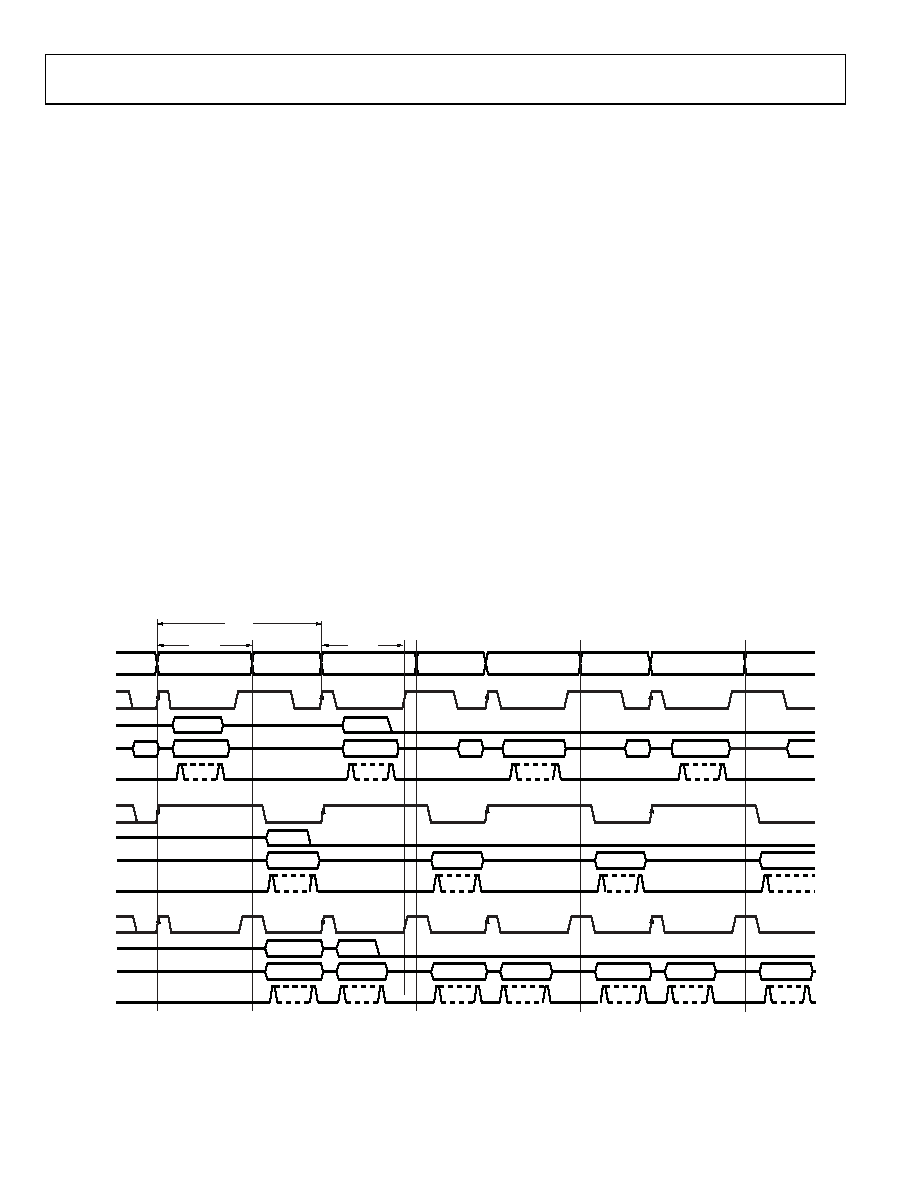
Figure 39 details the timing for all three modes without a busy
indicator. Refer to the Read/Write Spanning Conversion
Without a Busy Indicator section and the Read/Write Spanning
Conversion Without a Busy Indicator section for more details.
The sequencer can also be used with the busy indicator and
details for these timings can be found in the General Timing
with a Busy Indicator section and the Read/Write Spanning
Conversion with a Busy Indicator section.
For sequencer operation, the CFG register should be set during
the (n 1) phase after power-up. On phase (n), the sequencer
setting takes place and acquires IN0. The first valid conversion
result is available at phase (n + 1). After the last channel set in
CFG[9:7] is converted, the internal temperature sensor data is
output (if enabled), followed by acquisition of IN0.
Examples
With all channels configured for unipolar mode to GND,
including the internal temperature sensor, the sequence scans in
the following order:
IN0, IN1, IN2, IN3, IN4, IN5, IN6, IN7, TEMP, IN0, IN1, IN2, …
For paired channels with the internal temperature sensor
enabled, the sequencer scans in the following order:
IN0, IN2, IN4, IN6, TEMP, IN0, …
Note that IN1, IN3, IN5, and IN7 are referenced to a GND
ACQUISITION
(n – 1) UNDEFINED
ACQUISITION
(n), IN0
ACQUISITION
(n + 1), IN1
ACQUISITION
(n + 2), IN2
PHASE
POWER
UP
EOC
SOC
EOC
CONVERSION
(n – 1) UNDEFINED
CONVERSION
(n), IN0
CONVERSION
(n + 1), IN1
CONVERSION
(n – 2) UNDEFINED
07
35
3-
0
4
6
tCONV
tCYC
tDATA
CNV
DIN
SDO
XXX
MSB
XXX
MSB
XXX
NOTES
1. CNV MUST BE HIGH PRIOR TO THE END OF CONVERSION (EOC) TO AVOID THE BUSY INDICATOR.
2. A TOTAL OF 16 SCK FALLING EDGES ARE REQUIRED TO RETURN SDO TO HIGH-Z. IF CFG READBACK IS ENABLED,
A TOTAL OF 30 SCK FALLING EDGES IS REQUIRED TO RETURN SDO TO HIGH-Z.
DATA IN0
DATA (n – 1)
XXX
DATA (n – 1)
XXX
DATA (n – 1)
XXX
DATA (n – 1)
XXX
DATA (n – 2)
XXX
DATA (n – 2)
XXX
DATA (n – 2)
XXX
DATA (n – 2)
XXX
DATA (n – 3)
XXX
MSB
IN0
MSB
IN1
DIN
SDO
DATA IN1
DATA IN0
DATA IN1
DIN
CFG (n)
SDO
SCK
1
NOTE 1
16
NOTE 2
2
1
SCK
116
16
nn
n
n + 1
n
1
SCK
1
116
16
1
CFG (n)
RDC
RAC
RSC
CFG (n)
Figure 39. General Channel Sequencer Timing Without a Busy Indicator
相关PDF资料 |
PDF描述 |
|---|---|
| AD7794BRUZ | IC ADC 24BIT SIG-DEL 6CH 24TSSOP |
| AD7689ACPZ | IC ADC 16BIT 250KSPS 8CH 20LFCSP |
| LTC1598CG#PBF | IC A/D CONV 12BIT SRL 8CH 24SSOP |
| KA339A | IC COMPARATOR QUAD 14-DIP |
| KA339 | IC COMPARATOR QUAD 14-DIP |
相关代理商/技术参数 |
参数描述 |
|---|---|
| AD7682BCPZRL7 | 功能描述:IC ADC 16BIT 4CH 250KSPS 20LFCSP RoHS:是 类别:集成电路 (IC) >> 数据采集 - 模数转换器 系列:PulSAR® 标准包装:1,000 系列:- 位数:16 采样率(每秒):45k 数据接口:串行 转换器数目:2 功率耗散(最大):315mW 电压电源:模拟和数字 工作温度:0°C ~ 70°C 安装类型:表面贴装 封装/外壳:28-SOIC(0.295",7.50mm 宽) 供应商设备封装:28-SOIC W 包装:带卷 (TR) 输入数目和类型:2 个单端,单极 |
| AD7683 | 制造商:AD 制造商全称:Analog Devices 功能描述:16-Bit, 100 kSPS PulSAR ADC in MSOP/QFN |
| AD7683ACPZRL | 功能描述:IC ADC 16BIT SRL 100KSPS 8LFCSP RoHS:是 类别:集成电路 (IC) >> 数据采集 - 模数转换器 系列:PulSAR® 标准包装:1,000 系列:- 位数:16 采样率(每秒):45k 数据接口:串行 转换器数目:2 功率耗散(最大):315mW 电压电源:模拟和数字 工作温度:0°C ~ 70°C 安装类型:表面贴装 封装/外壳:28-SOIC(0.295",7.50mm 宽) 供应商设备封装:28-SOIC W 包装:带卷 (TR) 输入数目和类型:2 个单端,单极 |
| AD7683ACPZRL7 | 功能描述:IC ADC 16BIT 100KSPS 8LFCSP RoHS:是 类别:集成电路 (IC) >> 数据采集 - 模数转换器 系列:PulSAR® 标准包装:1,000 系列:- 位数:16 采样率(每秒):45k 数据接口:串行 转换器数目:2 功率耗散(最大):315mW 电压电源:模拟和数字 工作温度:0°C ~ 70°C 安装类型:表面贴装 封装/外壳:28-SOIC(0.295",7.50mm 宽) 供应商设备封装:28-SOIC W 包装:带卷 (TR) 输入数目和类型:2 个单端,单极 |
| AD7683ARM | 制造商:Analog Devices 功能描述:ADC Single SAR 100ksps 16-bit Serial 8-Pin MSOP Tube |
发布紧急采购,3分钟左右您将得到回复。