- 您现在的位置:买卖IC网 > PDF目录10300 > AD7707BRZ-REEL (Analog Devices Inc)IC ADC 16BIT 3CHAN 20SOIC PDF资料下载
参数资料
| 型号: | AD7707BRZ-REEL |
| 厂商: | Analog Devices Inc |
| 文件页数: | 18/52页 |
| 文件大小: | 0K |
| 描述: | IC ADC 16BIT 3CHAN 20SOIC |
| 标准包装: | 1,000 |
| 位数: | 16 |
| 采样率(每秒): | 500 |
| 数据接口: | DSP,MICROWIRE?,QSPI?,串行,SPI? |
| 转换器数目: | 1 |
| 功率耗散(最大): | 1mW |
| 电压电源: | 模拟和数字 |
| 工作温度: | -40°C ~ 85°C |
| 安装类型: | 表面贴装 |
| 封装/外壳: | 20-SOIC(0.295",7.50mm 宽) |
| 供应商设备封装: | 20-SOIC W |
| 包装: | 带卷 (TR) |
| 输入数目和类型: | 1 个单端,单极;1 个单端,双极;2 个伪差分,单极;2 个伪差分,双极 |
第1页第2页第3页第4页第5页第6页第7页第8页第9页第10页第11页第12页第13页第14页第15页第16页第17页当前第18页第19页第20页第21页第22页第23页第24页第25页第26页第27页第28页第29页第30页第31页第32页第33页第34页第35页第36页第37页第38页第39页第40页第41页第42页第43页第44页第45页第46页第47页第48页第49页第50页第51页第52页
AD7707
Rev. B | Page 25 of 52
ANALOG INPUT
ANALOG INPUT RANGES
The AD7707 contains two low level pseudo differential analog
input channels, AIN1 and AIN2. These input pairs provide
programmable-gain, differential input channels that can handle
either unipolar or pseudo bipolar input signals. It should be
noted that the bipolar input signals are referenced to the LOCOM
input. The AD7707 also has a high level analog input channel
AIN3, which is referenced to HICOM. Figure 13 shows the input
structure on the high level input channel.
In normal 5 V operation, VBIAS is normally connected to 2.5 V
and HICOM is connected to AGND. This arrangement ensures
that the voltages seen internally are within the common-mode
range of the buffer in buffered mode and within the supply range in
unbuffered mode. This device can be programmed to operate in
either buffered or unbuffered mode via the BUF bit in the setup
register. Note that the signals on AIN3 are with respect to the
HICOM input and not with respect to AGND or DGND.
The differential voltage seen by the AD7707 when using the
high level input channel is the difference between AIN3(+) and
AIN3() on the mux as shown in Figure 13.
AIN3(+) = (AIN3 + 6 × VBIAS + VHICOM)/8
1R
AIN3(+)
AIN3(–)
AIN3
VBIAS
HICOM
3R
6R
MUX
6R
1R = 5k
08
69
1-
0
13
Figure 13. AIN3 Input Structure
AIN3() = VHICOM + 0.75 × (VBIAS VHICOM)
In unbuffered mode, the common-mode range of the low level
input channels is from AGND 100 mV to AVDD + 30 mV. This
means that in unbuffered mode, the part can handle both unipolar
and bipolar input ranges for all gains. Absolute voltages of
AGND 100 mV can be accommodated on the analog inputs
without degradation in performance, but leakage current increases
appreciably with increasing temperature. In buffered mode, the
analog inputs can handle much larger source impedances, but
the absolute input voltage range is restricted to between AGND
+ 50 mV to AVDD 1.5 V, which also places restrictions on the
common-mode range. This means that in buffered mode, there
are some restrictions on the allowable gains for bipolar input
ranges. Care must be taken in setting up the common-mode
voltage and input voltage range so that these limits are not
exceeded; otherwise, there will be a degradation in linearity
performance.
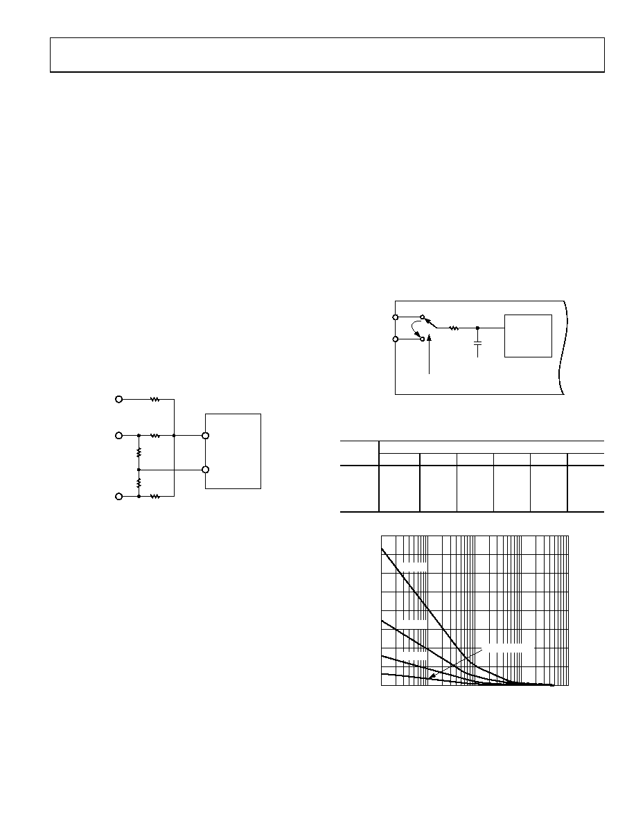
In unbuffered mode, the analog inputs look directly into the 7 pF
input sampling capacitor, CSAMP. The dc input leakage current in
this unbuffered mode is 1 nA maximum. As a result, the analog
inputs see a dynamic load that is switched at the input sample
rate (see Figure 14). This sample rate depends on master clock
frequency and selected gain. CSAMP is charged to AIN(+) and
discharged to AIN() every input sample cycle. The effective
resistance of the switch, RSW, is typically 7 kΩ.
CSAMP must be charged through RSW and any additional source
impedances every input sample cycle. Therefore, in unbuffered
mode, source impedances mean a longer charge time for CSAMP
and this may result in gain errors on the part. Table 26 shows
the allowable external resistance/capacitance values, for unbuffered
mode, such that no gain error to the 16-bit level is introduced
on the part. Note that these capacitances are total capacitances
on the analog input. This external capacitance includes 10 pF
from the pins and lead frame of the device.
08
69
1-
01
4
AIN(+)
AIN(–)
FIRST
INTEGRATOR
HIGH INPUT
IMPEDANCE
>1G
RSW (7k TYP)
SWITCHING FREQUENCY DEPENDS ON
fCLKIN AND SELECTED GAIN
CSAMP
(7pF)
VDD/2
Figure 14. Unbuffered Analog Input Structure
Table 26. External R, C Combination for No 16-Bit Gain
Error on Low Level Input Channels (Unbuffered Mode Only)
External Capacitance (pF)
Gain
0
50
100
500
1000
5000
1
368 kΩ
90.6 kΩ
54.2 kΩ
14.6 kΩ
8.2 kΩ
2.2 kΩ
2
177.2 kΩ
44.2 kΩ
26.4 kΩ
7.2 kΩ
4 kΩ
1.12 kΩ
4
82.8 kΩ
21.2 kΩ
12.6 kΩ
3.4 kΩ
1.94 kΩ
540 Ω
8 to 128
35.2 kΩ
9.6 kΩ
5.8 kΩ
1.58 Ω
880 Ω
240 Ω
EXTERNAL CAPACITANCE (pF)
0
10000
E
X
T
E
RNAL
RE
S
IS
T
ANCE
(
k
)
10
100
1000
0
50
100
150
200
250
300
350
400
GAIN = 1
GAIN = 4
GAIN = 8 TO 128
GAIN = 2
08
69
1-
01
5
Figure 15. External R, C Combination for No 16-Bit Gain Error on Low Level
Input Channels (Unbuffered Mode Only)
相关PDF资料 |
PDF描述 |
|---|---|
| MS27468T25B46B | CONN HSG RCPT 46POS JAMNUT SCKT |
| LTC2366CS6#TRPBF | IC ADC 12BIT 3MSPS TSOT23-6 |
| LTC1404IS8#PBF | IC A/D CONV 12BIT W/SHTDN 8-SOIC |
| MS27468E25B46B | CONN HSG RCPT 46POS JAMNUT SCKT |
| LTC1404IS8 | IC A/D CONV 12BIT W/SHTDN 8-SOIC |
相关代理商/技术参数 |
参数描述 |
|---|---|
| AD7707BRZ-REEL7 | 功能描述:IC ADC 16BIT 3CHAN 20SOIC RoHS:是 类别:集成电路 (IC) >> 数据采集 - 模数转换器 系列:- 标准包装:1,000 系列:- 位数:16 采样率(每秒):45k 数据接口:串行 转换器数目:2 功率耗散(最大):315mW 电压电源:模拟和数字 工作温度:0°C ~ 70°C 安装类型:表面贴装 封装/外壳:28-SOIC(0.295",7.50mm 宽) 供应商设备封装:28-SOIC W 包装:带卷 (TR) 输入数目和类型:2 个单端,单极 |
| AD7707EB | 制造商:AD 制造商全称:Analog Devices 功能描述:3 V/5 V 610 V Input Range 1 mW 3-Channel 16-Bit Sigma-Delta ADC(316.51 k) |
| AD7708 | 制造商:AD 制造商全称:Analog Devices 功能描述:8-/10-Channel, Low Voltage, Low Power, ADCs |
| AD7708BR | 功能描述:IC ADC 16BIT R-R 8/10CH 28-SOIC RoHS:否 类别:集成电路 (IC) >> 数据采集 - 模数转换器 系列:- 标准包装:1,000 系列:- 位数:16 采样率(每秒):45k 数据接口:串行 转换器数目:2 功率耗散(最大):315mW 电压电源:模拟和数字 工作温度:0°C ~ 70°C 安装类型:表面贴装 封装/外壳:28-SOIC(0.295",7.50mm 宽) 供应商设备封装:28-SOIC W 包装:带卷 (TR) 输入数目和类型:2 个单端,单极 |
| AD7708BR-REEL | 功能描述:IC ADC 16BIT R-R 8/10CH 28-SOIC RoHS:否 类别:集成电路 (IC) >> 数据采集 - 模数转换器 系列:- 标准包装:1,000 系列:- 位数:16 采样率(每秒):45k 数据接口:串行 转换器数目:2 功率耗散(最大):315mW 电压电源:模拟和数字 工作温度:0°C ~ 70°C 安装类型:表面贴装 封装/外壳:28-SOIC(0.295",7.50mm 宽) 供应商设备封装:28-SOIC W 包装:带卷 (TR) 输入数目和类型:2 个单端,单极 |
发布紧急采购,3分钟左右您将得到回复。