- 您现在的位置:买卖IC网 > PDF目录10239 > AD7714YRZ-REEL (Analog Devices Inc)IC ADC 24BIT SIGMA-DELTA 24SOIC PDF资料下载
参数资料
| 型号: | AD7714YRZ-REEL |
| 厂商: | Analog Devices Inc |
| 文件页数: | 22/40页 |
| 文件大小: | 0K |
| 描述: | IC ADC 24BIT SIGMA-DELTA 24SOIC |
| 标准包装: | 1,000 |
| 位数: | 24 |
| 采样率(每秒): | 1k |
| 数据接口: | DSP,MICROWIRE?,QSPI?,串行,SPI? |
| 转换器数目: | 1 |
| 功率耗散(最大): | 7mW |
| 电压电源: | 模拟和数字 |
| 工作温度: | -40°C ~ 105°C |
| 安装类型: | 表面贴装 |
| 封装/外壳: | 24-SOIC(0.295",7.50mm 宽) |
| 供应商设备封装: | 24-SOIC W |
| 包装: | 带卷 (TR) |
| 输入数目和类型: | 3 个差分,单极;3 个差分,双极;5 个伪差分,单极;5 个伪差分,双极 |
| 配用: | EVAL-AD7714-3EBZ-ND - BOARD EVAL FOR AD7714 |
第1页第2页第3页第4页第5页第6页第7页第8页第9页第10页第11页第12页第13页第14页第15页第16页第17页第18页第19页第20页第21页当前第22页第23页第24页第25页第26页第27页第28页第29页第30页第31页第32页第33页第34页第35页第36页第37页第38页第39页第40页
2
AD7714
REV. C
–29–
DIGITAL INTERFACE
The AD7714’s programmable functions are controlled using a
set of on-chip registers as previously outlined. Data is written to
these registers via the part’s serial interface, and read access to
the on-chip registers is also provided by this interface. All com-
munications to the part must start with a write operation to the
Communications Register. After power-on or
RESET, the de-
vice expects a write to its Communications Register. The data
written to this register determines whether the next operation to
the part is a read or a write operation and also determines to
which register this read or write operation occurs. Therefore,
write access to any of the other registers on the part starts with a
write operation to the Communications Register followed by a
write to the selected register. A read operation from any register
on the part (including the output data register) starts with a
write operation to the Communications Register followed by a
read operation from the selected register.
The AD7714’s serial interface consists of five signals,
CS,
SCLK, DIN, DOUT and
DRDY. The DIN line is used for
transferring data into the on-chip registers while the DOUT line
is used for accessing data from the on-chip registers. SCLK is
the serial clock input for the device and all data transfers (either
on DIN or DOUT) take place with respect to this SCLK signal.
The
DRDY line is used as a status signal to indicate when data
is ready to be read from the AD7714’s data register.
DRDY
goes low when a new data word is available in the output regis-
ter. It is reset high when a read operation from the data register
is complete. It also goes high prior to the updating of the output
register to indicate when not to read from the device to ensure
that a data read is not attempted while the register is being
updated.
CS is used to select the device. It can be used to de-
code the AD7714 in systems where a number of parts are con-
nected to the serial bus.
The AD7714 serial interface can operate in three-wire mode by
tying the
CS input low. In this case, the SCLK, DIN and
DOUT lines are used to communicate with the AD7714 and
the status of
DRDY can be obtained by interrogating the MSB
of the Communications Register.
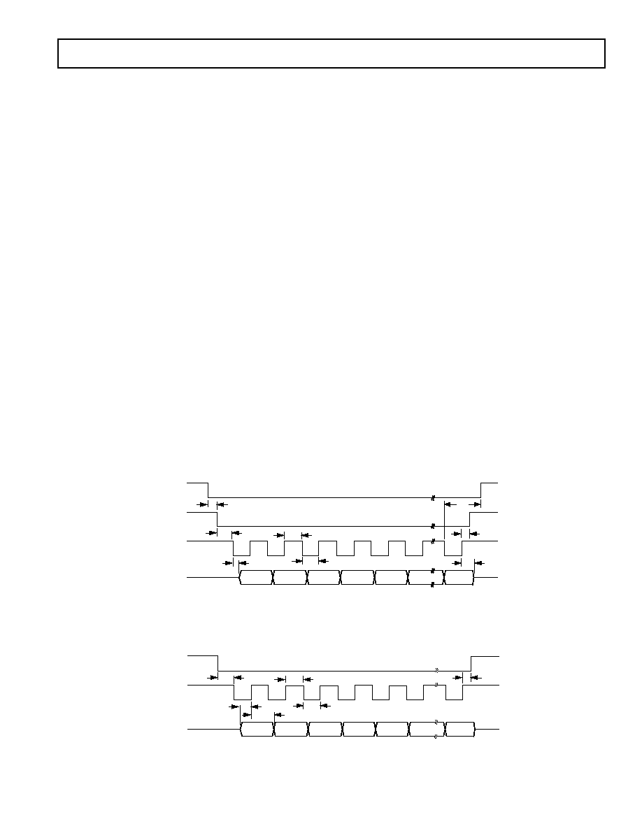
Figures 6 and 7 show timing diagrams for interfacing to the
AD7714 with
CS used to decode the part. Figure 6 is for a read
operation from the AD7714’s output shift register, while Figure
7 shows a write operation to the input shift register. Both dia-
grams are for the POL input at a logic high; for operation with
the POL input at a logic low simply invert the SCLK waveform
shown in the diagrams. It is possible to read the same data
twice from the output register even though the
DRDY line
returns high after the first read operation. Care must be taken,
however, to ensure that the read operations have been com-
pleted before the next output update is about to take place.
The serial interface can be reset by exercising the
RESET input
on the part. It can also be reset by writing a series of 1s on the
DIN input. If a logic 1 is written to the AD7714 DIN line for at
least 32 serial clock cycles the serial interface is reset. This
ensures in three-wire systems that if the interface gets lost, either
via a software error or by some glitch in the system, it can be
reset back into a known state. This state returns the interface to
where the AD7714 is expecting a write operation to the Com-
munications Register. This operation does not in itself reset the
contents of any registers but since the interface was lost, the
information that was written to any of the registers is unknown
and it is advisable to set up all registers again.
Figure 6. Read Cycle Timing Diagram (POL = 1)
Figure 7. Write Cycle Timing Diagram (POL = 1)
DOUT
SCLK
CS
DRDY
MSB
t5
t7
t9
LSB
t8
t6
t4
t3
t10
DIN
SCLK
CS
MSB
t12
t15
LSB
t16
t14
t11
t13
相关PDF资料 |
PDF描述 |
|---|---|
| VI-23B-CU-F3 | CONVERTER MOD DC/DC 95V 200W |
| VI-B7Z-MW | CONVERTER MOD DC/DC 2V 40W |
| VE-B2V-MW-F3 | CONVERTER MOD DC/DC 5.8V 100W |
| VI-23B-CU-F2 | CONVERTER MOD DC/DC 95V 200W |
| VI-234-IW-S | CONVERTER MOD DC/DC 48V 100W |
相关代理商/技术参数 |
参数描述 |
|---|---|
| AD7714YRZ-REEL7 | 功能描述:IC ADC 24BIT SIGMA-DELTA 24SOIC RoHS:是 类别:集成电路 (IC) >> 数据采集 - 模数转换器 系列:- 标准包装:1,000 系列:- 位数:12 采样率(每秒):300k 数据接口:并联 转换器数目:1 功率耗散(最大):75mW 电压电源:单电源 工作温度:0°C ~ 70°C 安装类型:表面贴装 封装/外壳:24-SOIC(0.295",7.50mm 宽) 供应商设备封装:24-SOIC 包装:带卷 (TR) 输入数目和类型:1 个单端,单极;1 个单端,双极 |
| AD7715 | 制造商:AD 制造商全称:Analog Devices 功能描述:3 V/5 V, 450 uA 16-Bit, Sigma-Delta ADC |
| AD7715_10 | 制造商:AD 制造商全称:Analog Devices 功能描述:3 V/5 V, 450 ??A 16-Bit, Sigma-Delta ADC |
| AD7715-5EB | 制造商:Analog Devices 功能描述: |
发布紧急采购,3分钟左右您将得到回复。