- 您现在的位置:买卖IC网 > PDF目录10239 > AD7714YRZ-REEL (Analog Devices Inc)IC ADC 24BIT SIGMA-DELTA 24SOIC PDF资料下载
参数资料
| 型号: | AD7714YRZ-REEL |
| 厂商: | Analog Devices Inc |
| 文件页数: | 6/40页 |
| 文件大小: | 0K |
| 描述: | IC ADC 24BIT SIGMA-DELTA 24SOIC |
| 标准包装: | 1,000 |
| 位数: | 24 |
| 采样率(每秒): | 1k |
| 数据接口: | DSP,MICROWIRE?,QSPI?,串行,SPI? |
| 转换器数目: | 1 |
| 功率耗散(最大): | 7mW |
| 电压电源: | 模拟和数字 |
| 工作温度: | -40°C ~ 105°C |
| 安装类型: | 表面贴装 |
| 封装/外壳: | 24-SOIC(0.295",7.50mm 宽) |
| 供应商设备封装: | 24-SOIC W |
| 包装: | 带卷 (TR) |
| 输入数目和类型: | 3 个差分,单极;3 个差分,双极;5 个伪差分,单极;5 个伪差分,双极 |
| 配用: | EVAL-AD7714-3EBZ-ND - BOARD EVAL FOR AD7714 |
第1页第2页第3页第4页第5页当前第6页第7页第8页第9页第10页第11页第12页第13页第14页第15页第16页第17页第18页第19页第20页第21页第22页第23页第24页第25页第26页第27页第28页第29页第30页第31页第32页第33页第34页第35页第36页第37页第38页第39页第40页
AD7714
REV. C
–14–
ON-CHIP REGISTERS
The AD7714 contains eight on-chip registers which can be accessed via the serial port of the part. The first of these is a Communica-
tions Register which controls the channel selection, decides whether the next operation is a read or write operation and also decides
which register the next read or write operation accesses. All communications to the part must start with a write operation to the
Communications Register. After power-on or
RESET, the device expects a write to its Communications Register. The data written
to this register determines whether the next operation to the part is a read or a write operation and also determines to which register
this read or write operation occurs. Therefore, write access to any of the other registers on the part starts with a write operation to the
Communications Register followed by a write to the selected register. A read operation from any other register on the part (including
the output data register) starts with a write operation to the Communications Register followed by a read operation from the selected
register. The communications register also controls channel selection and the
DRDY status is also available by reading from the
Communications Register. The second register is a Mode Register which determines calibration mode and gain setting. The third
register is labelled the Filter High Register and this determines the word length, bipolar/unipolar operation and contains the upper 4
bits of the filter selection word. The fourth register is labelled the Filter Low Register and contains the lower 8 bits of the filter selec-
tion word. The fifth register is a Test Register which is accessed when testing the device. The sixth register is the Data Register from
which the output data from the part is accessed. The final registers allow access to the part’s calibration registers. The Zero Scale
Calibration Register allows access to the zero scale calibration coefficients for the selected input channel while the Full Scale Calibra-
tion Register allows access to the full scale calibration coefficients for the selected input channel. The registers are discussed in more
detail in the following sections.
Communications Register (RS2-RS0 = 0, 0, 0)
The Communications Register is an 8-bit register from which data can either be read or to which data can be written. All communi-
cations to the part must start with a write operation to the Communications Register. The data written to the Communications Reg-
ister determines whether the next operation is a read or write operation and to which register this operation takes place. Once the
subsequent read or write operation to the selected register is complete, the interface returns to where it expects a write operation to
the Communications Register. This is the default state of the interface, and on power-up or after a
RESET, the AD7714 is in this
default state waiting for a write operation to the Communications Register. In situations where the interface sequence is lost, if a
write operation of sufficient duration (containing at least 32 serial clock cycles) takes place with DIN high, the AD7714 returns to
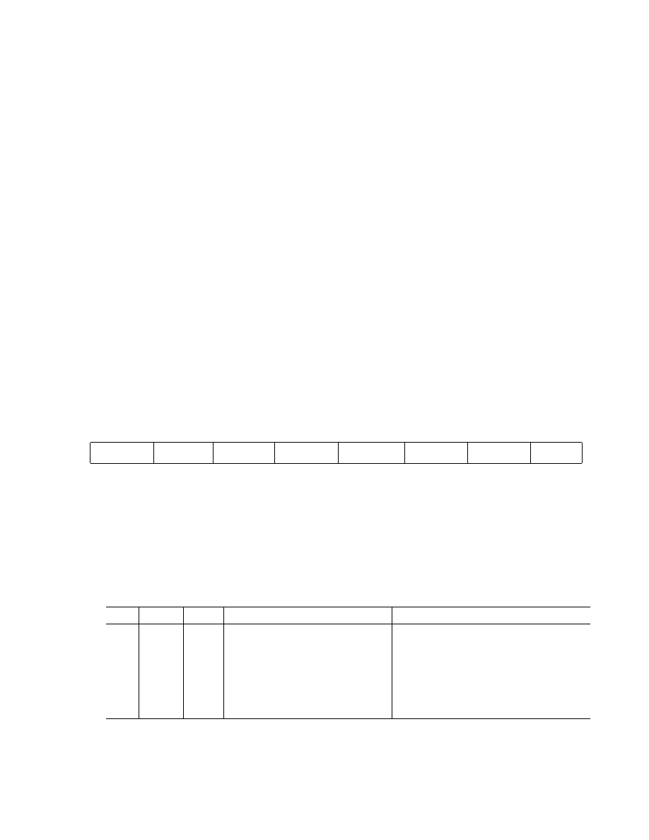
this default state. Table V outlines the bit designations for the Communications Register.
Table V. Communications Register
Table VI. Register Selection
0/
DRDY
RS2
RS1
RS0
R/
W
CH2
CH1
CH0
0/
DRDY
For a write operation, a 0 must be written to this bit so that the write operation to the Communications Register
actually takes place. If a 1 is written to this bit, the part will not clock on to subsequent bits in the register. It will stay
at this bit location until a 0 is written to this bit. Once a 0 is written to this bit, the next 7 bits will be loaded to the
Communications Register. For a read operation, this bit provides the status of the
DRDY flag from the part. The
status of this bit is the same as the
DRDY output pin.
RS2–RS0
Register Selection Bits. RS2 is the MSB of the three selection bits. The three bits select to which one of eight on-chip
registers the next read or write operation takes place as shown in Table VI along with the register size.
RS2
RS1
RS0
Register
Register Size
0
Communications Register
8 Bits
0
1
Mode Register
8 Bits
0
1
0
Filter High Register
8 Bits
0
1
Filter Low Register
8 Bits
1
0
Test Register
8 Bits
1
0
1
Data Register
16 Bits or 24 Bits
1
0
Zero-Scale Calibration Register
24 Bits
1
Full-Scale Calibration Register
24 Bits
相关PDF资料 |
PDF描述 |
|---|---|
| VI-23B-CU-F3 | CONVERTER MOD DC/DC 95V 200W |
| VI-B7Z-MW | CONVERTER MOD DC/DC 2V 40W |
| VE-B2V-MW-F3 | CONVERTER MOD DC/DC 5.8V 100W |
| VI-23B-CU-F2 | CONVERTER MOD DC/DC 95V 200W |
| VI-234-IW-S | CONVERTER MOD DC/DC 48V 100W |
相关代理商/技术参数 |
参数描述 |
|---|---|
| AD7714YRZ-REEL7 | 功能描述:IC ADC 24BIT SIGMA-DELTA 24SOIC RoHS:是 类别:集成电路 (IC) >> 数据采集 - 模数转换器 系列:- 标准包装:1,000 系列:- 位数:12 采样率(每秒):300k 数据接口:并联 转换器数目:1 功率耗散(最大):75mW 电压电源:单电源 工作温度:0°C ~ 70°C 安装类型:表面贴装 封装/外壳:24-SOIC(0.295",7.50mm 宽) 供应商设备封装:24-SOIC 包装:带卷 (TR) 输入数目和类型:1 个单端,单极;1 个单端,双极 |
| AD7715 | 制造商:AD 制造商全称:Analog Devices 功能描述:3 V/5 V, 450 uA 16-Bit, Sigma-Delta ADC |
| AD7715_10 | 制造商:AD 制造商全称:Analog Devices 功能描述:3 V/5 V, 450 ??A 16-Bit, Sigma-Delta ADC |
| AD7715-5EB | 制造商:Analog Devices 功能描述: |
发布紧急采购,3分钟左右您将得到回复。