参数资料
| 型号: | AD7760BSVZ-REEL |
| 厂商: | Analog Devices Inc |
| 文件页数: | 28/37页 |
| 文件大小: | 0K |
| 描述: | IC ADC 24BIT 2.5MSPS 64TQFP |
| 标准包装: | 1,500 |
| 位数: | 24 |
| 采样率(每秒): | 2.5M |
| 数据接口: | 并联 |
| 转换器数目: | 1 |
| 功率耗散(最大): | 958mW |
| 电压电源: | 模拟和数字 |
| 工作温度: | -40°C ~ 85°C |
| 安装类型: | 表面贴装 |
| 封装/外壳: | 64-TQFP 裸露焊盘 |
| 供应商设备封装: | 64-TQFP-EP(10x10) |
| 包装: | 带卷 (TR) |
| 输入数目和类型: | 1 个差分,单极;1 个差分,双极 |
第1页第2页第3页第4页第5页第6页第7页第8页第9页第10页第11页第12页第13页第14页第15页第16页第17页第18页第19页第20页第21页第22页第23页第24页第25页第26页第27页当前第28页第29页第30页第31页第32页第33页第34页第35页第36页第37页
AD7760
Rev. A | Page 33 of 36
AD7760 REGISTERS
The AD7760 has a number of user-programmable registers. The control registers are used to set the decimation rate, the filter configuration, the
clock divider, and so on. There are also digital gain, offset, and overrange threshold registers. Writing to these registers involves writing
the register address first, then a 16-bit data-word. Register addresses, details of individual bits, and default values are given in this section.
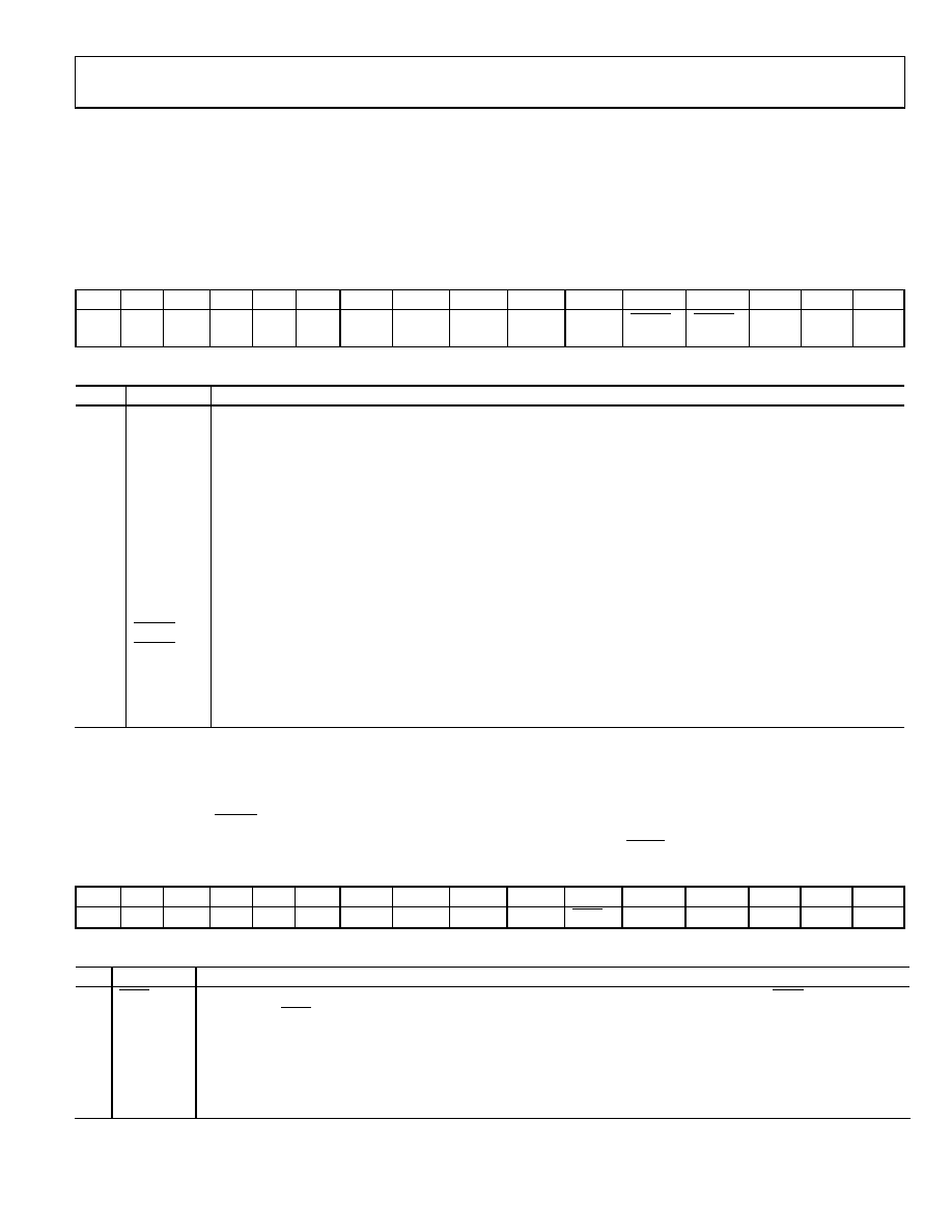
CONTROL REGISTER 1—ADDRESS 0x0001
Default Value 0x001A
MSB
LSB
D15
D14
D13
D12
D11
D10
D9
D8
D7
D6
D5
D4
D3
D2
D1
D0
DL_
FILT
RD
OVR
RD
GAIN
RD
OFF
RD
STAT
0
SYNC
FLEN3
FLEN2
FLEN1
FLEN0
BYP F3
BYP F1
DEC2
DEC1
DEC0
Table 15. Bit Descriptions of Control Register 1
Bit
Mnemonic
Description
15
DL_FILT1
Download Filter. Before downloading a user-defined filter, this bit must be set. The filter length bits must
also be set at this time. The write operations that follow are interpreted as the user coefficients for the FIR
filter until all the coefficients and the checksum have been written.
14
RD OVR1, 2
Read Overrange. If this bit has been set, the next read operation outputs the contents of the overrange
threshold register instead of a conversion result.
13
RD GAIN1, 2
Read Gain. If this bit has been set, the next read operation outputs the contents of the digital gain register.
12
RD OFF1, 2
Read Offset. If this bit has been set, the next read operation outputs the contents of the digital offset register.
11
RD STAT1, 2
Read Status. If this bit has been set, the next read operation outputs the contents of the status register.
10
0
0 must be written to this bit.
9
SYNC1
Synchronize. Setting this bit initiates an internal synchronization routine. Setting this bit simultaneously on
multiple devices synchronizes all filters.
8 to 5
FLEN [3:0]
Filter Length Bits. These bits must be set when the DL_FILT bit is set before a user-defined filter is downloaded.
4
BYP F3
Bypass Filter 3. If this bit is 0, Filter 3 (programmable FIR) is bypassed.
3
BYP F1
Bypass Filter 1. If this bit is 0, Filter 1 is bypassed. This should only occur when the user requires unfiltered
modulator data to be output.
2 to 0
DEC [2:0]
Decimation Rate. These bits set the decimation rate of Filter 2. All 0s implies that the filter is bypassed. A value
of 1 corresponds to 2× decimation, a value of 2 corresponds to 4× decimation, and so on, up to the maximum
value of 5, corresponding to 32× decimation.
1 Bit 15 to Bit 9 are self-clearing bits.
2 Only one of the bits from Bit 14 to Bit 11 can be set in any write operation because it determines the contents of the next read operation.
CONTROL REGISTER 2—ADDRESS 0x0002
Default Value After RESET: 0x009B
Recommended register setting for power-up and normal operation using clock divide-by-2 (CDIV = 0) mode: 0x0002
MSB
LSB
D15
D14
D13
D12
D11
D10
D9
D8
D7
D6
D5
D4
D3
D2
D1
D0
0
CDIV
0
PD
LPWR
1
D1PD
Table 16. Bit Descriptions of Control Register 2
Bit
Mnemonic
Description
5
CDIV
Clock Divider Bit. This sets the divide ratio of the MCLK signal to produce the internal ICLK. Setting CDIV = 0 divides the
MCLK by 2. If CDIV = 1, the ICLK frequency is equal to the MCLK.
3
PD
Power Down. Setting this bit powers down the AD7760, reducing the power consumption to 6.35 mW.
2
LPWR
Low Power. If this bit is set, the AD7760 is operating in a low power mode. The power consumption is reduced for a 6 dB
reduction in noise performance.
1
Write 1 to this bit.
0
D1PD
Differential Amplifier Power Down. Setting this bit powers down the on-chip differential amplifier.
相关PDF资料 |
PDF描述 |
|---|---|
| AD7762BSVZ-REEL | IC ADC 24BIT 625KSPS 64TQFP |
| AD7763BSVZ | IC ADC 24BIT SRL 625KSPS 64TQFP |
| AD7764BRUZ-REEL7 | IC ADC 24BIT S/D 312KSPS 28TSSOP |
| AD7765BRUZ-REEL7 | IC ADC 24BIT S/D 156KSPS 28TSSOP |
| AD7766BRUZ-RL7 | IC ADC 24BIT 128KSPS SAR 16TSSOP |
相关代理商/技术参数 |
参数描述 |
|---|---|
| AD7761BSTZ | 功能描述:16 Bit Analog to Digital Converter 8 Input 8 Sigma-Delta 64-LQFP (10x10) 制造商:analog devices inc. 系列:- 包装:托盘 零件状态:有效 位数:16 采样率(每秒):256k 输入数:8 输入类型:差分 数据接口:SPI 配置:ADC 无线电 - S/H:ADC:- A/D 转换器数:8 架构:三角积分 参考类型:外部 电压 - 电源,模拟:2 V ~ 5.5 V 电压 - 电源,数字:- 特性:同步采样 工作温度:-40°C ~ 105°C 封装/外壳:64-LQFP 供应商器件封装:64-LQFP(10x10) 标准包装:1 |
| AD7761BSTZ-RL | 功能描述:16 Bit Analog to Digital Converter 8 Input 8 Sigma-Delta 64-LQFP (10x10) 制造商:analog devices inc. 系列:- 包装:带卷(TR) 零件状态:有效 位数:16 采样率(每秒):256k 输入数:8 输入类型:差分 数据接口:SPI 配置:ADC 无线电 - S/H:ADC:- A/D 转换器数:8 架构:三角积分 参考类型:外部 电压 - 电源,模拟:2 V ~ 5.5 V 电压 - 电源,数字:- 特性:同步采样 工作温度:-40°C ~ 105°C 封装/外壳:64-LQFP 供应商器件封装:64-LQFP(10x10) 标准包装:1,500 |
| AD7762 | 制造商:AD 制造商全称:Analog Devices 功能描述:24-Bit, 8.5 mW, 109 dB, 128/64/32 kSPS ADCs |
| AD77628SVZ | 制造商:Analog Devices 功能描述: |
| AD7762BCP | 制造商:Analog Devices 功能描述:ADC SGL DELTA-SIGMA 625KSPS 24BIT PARALLEL 48LFCSP - Bulk |
发布紧急采购,3分钟左右您将得到回复。