- 您现在的位置:买卖IC网 > PDF目录10211 > AD7858LANZ (Analog Devices Inc)IC ADC 12BIT 8CHAN SRL 24DIP PDF资料下载
参数资料
| 型号: | AD7858LANZ |
| 厂商: | Analog Devices Inc |
| 文件页数: | 11/32页 |
| 文件大小: | 0K |
| 描述: | IC ADC 12BIT 8CHAN SRL 24DIP |
| 标准包装: | 15 |
| 位数: | 12 |
| 采样率(每秒): | 100k |
| 数据接口: | 8051,QSPI?,串行,SPI? µP |
| 转换器数目: | 2 |
| 功率耗散(最大): | 33mW |
| 电压电源: | 模拟和数字 |
| 工作温度: | -40°C ~ 85°C |
| 安装类型: | 通孔 |
| 封装/外壳: | 24-DIP(0.300",7.62mm) |
| 供应商设备封装: | 24-PDIP |
| 包装: | 管件 |
| 输入数目和类型: | 8 个单端,单极;4 个伪差分,单极 |
第1页第2页第3页第4页第5页第6页第7页第8页第9页第10页当前第11页第12页第13页第14页第15页第16页第17页第18页第19页第20页第21页第22页第23页第24页第25页第26页第27页第28页第29页第30页第31页第32页
AD7858/AD7858L
REV. B
–19–
Table VI. Power Management Options
PMGT1 PMGT0
SLEEP
Bit
Pin
Comment
00
0
Full Power-Down if Not
Calibrating or Converting
(Default Condition
After Power-On)
00
1
Normal Operation
01
X
Normal Operation
(Independent of the
SLEEP Pin)
10
X
Full Power-Down
11
X
Partial Power-Down if Not
Converting
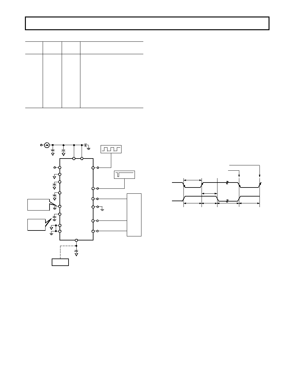
A typical connection diagram for a low power application is
shown in Figure 21 (AD7858L is the low power version of the
AD7858).
AUTO POWER
DOWN AFTER
CONVERSION
AUTO CAL
ON
POWER-UP
OPTIONAL
EXTERNAL
REFERENCE
1.8MHz
OSCILLATOR
MASTER
CLOCK
INPUT
0.1 F
10 F
ANALOG
SUPPLY
+3V
0V TO 2.5V
INPUT
0.1 F
0.01 F
0.1 F
INTERNAL
REFERENCE
100kHz
PULSE
GENERATOR
CONVERSION
START INPUT
SERIAL CLOCK
INPUT
SERIAL DATA
OUTPUT
CLKIN
SCLK
CONVST
SYNC
DIN
DOUT
DGND
AGND
CAL
SLEEP
CREF2
CREF1
AIN(–)
AIN(+)
AVDD DVDD
AD7858/
AD7858L
LOW
POWER
C/ P
CURRENT,
I = 1.5mA
TYP
SERIAL DATA
INPUT
REFIN /REFOUT
REF192
Figure 21. Typical Low Power Circuit
POWER-UP TIMES
Using an External Reference
When the AD7858 is powered up, the part is powered up from
one of two conditions. First, when the power supplies are ini-
tially powered up and, secondly, when the part is powered up
from either a hardware or software power-down (see last section).
When AVDD and DVDD are powered up, the AD7858 should be
left idle for approximately 32 ms (4 MHz CLK) to allow for the
autocalibration if a 10 nF cap is placed on the
CAL pin, (see
Calibration section). During power-up the functionality of the
SLEEP pin is disabled, i.e., the part will not power down until
the end of the calibration if
SLEEP is tied logic low. The auto-
calibration on power-up can be disabled if the
CAL pin is tied to
a logic high. If the autocalibration is disabled, then the user must
take into account the time required by the AD7858 to power-up
before a self-calibration is carried out. This power-up time is the
time taken for the AD7858 to power up when power is first
applied (300
s) typ) or the time it takes the external reference
to settle to the 12-bit level–whichever is the longer.
The AD7858 powers up from a full hardware or software
power-down in 5
s typ. This limits the throughput which the
part is capable of to 104 kSPS for the AD7858 operating with a
4 MHz CLK and 66 kSPS for the AD7858L with a 1.8 MHz
CLK when powering down between conversions. Figure 22
shows how power-down between conversions is implemented
using the
CONVST pin. The user first selects the power-down
between conversions option by using the
SLEEP pin and the
power management bits, PMGT1 and PMGT0, in the control
register, (see last section). In this mode the AD7858 automati-
cally enters a full power-down at the end of a conversion, i.e.,
when BUSY goes low. The falling edge of the next
CONVST
pulse causes the part to power up. Assuming the external refer-
ence is left powered up, the AD7858 should be ready for normal
operation 5
s after this falling edge. The rising edge of CONVST
initiates a conversion so the
CONVST pulse should be at least
5
s wide. The part automatically powers down on completion
of the conversion.
5 s
tCONVERT
POWER-UP
TIME
NORMAL
OPERATION
FULL
POWER-DOWN
POWER-UP
TIME
START CONVERSION ON RISING EDGE
POWER-UP ON FALLING EDGE
CONVST
BUSY
Figure 22. Power-Up Timing When Using
CONVST Pin
NOTE: Where the software CONVST is used or automatic full
power-down, the part must be powered up in software with an
extra write setting PMGT1 = 0 and PMGT0 = 1 before a con-
version is initiated in the next write. Automatic partial power-
down after a calibration is not possible; the part must be
powered down manually. If software calibrations are to be used
when operating in the partial power-down mode, then three
separate writes are required. The first initiates the type of cali-
bration required, the second write powers the part down into
partial power-down mode, while the third write powers the part
up again before the next calibration command is issued.
Using the Internal (On-Chip) Reference
As in the case of an external reference, the AD7858 can power-
up from one of two conditions, power-up after the supplies are
connected or power-up from hardware/software power-down.
When using the on-chip reference and powering up when AVDD
and DVDD are first connected, it is recommended that the power-
up calibration mode be disabled as explained above. When using
the on-chip reference, the power-up time is effectively the time
it takes to charge up the external capacitor on the REFIN/REFOUT
pin. This time is given by the equation:
tUP = 9
× R × C
where R
150 k and C = external capacitor.
相关PDF资料 |
PDF描述 |
|---|---|
| MS3102R28-21SW | CONN RCPT 37POS BOX MNT W/SCKT |
| A5FBXAU | CONN PLUG CORD FMAL 5PIN BLK/AU |
| MS3102E28-21SY | CONN RCPT 37POS BOX MNT W/SCKT |
| 15282-18PG-321 | CONN JACK 18POS CABLE PIN |
| SP3082EEN-L/TR | IC TXRX RS485/RS422 ESD 8NSOIC |
相关代理商/技术参数 |
参数描述 |
|---|---|
| AD7858LAR | 制造商:Analog Devices 功能描述:ADC Single SAR 100ksps 12-bit Serial 24-Pin SOIC W |
| AD7858LAR3 | 制造商:AD 制造商全称:Analog Devices 功能描述:3 V to 5 V Single Supply, 200 kSPS 8-Channel, 12-Bit Sampling ADC |
| AD7858LAR-REEL | 制造商:Analog Devices 功能描述:ADC Single SAR 100ksps 12-bit Serial 24-Pin SOIC W T/R |
| AD7858LARS | 功能描述:IC ADC 12BIT 8CH SRL 24-SSOP RoHS:否 类别:集成电路 (IC) >> 数据采集 - 模数转换器 系列:- 标准包装:1,000 系列:- 位数:12 采样率(每秒):300k 数据接口:并联 转换器数目:1 功率耗散(最大):75mW 电压电源:单电源 工作温度:0°C ~ 70°C 安装类型:表面贴装 封装/外壳:24-SOIC(0.295",7.50mm 宽) 供应商设备封装:24-SOIC 包装:带卷 (TR) 输入数目和类型:1 个单端,单极;1 个单端,双极 |
| AD7858LARS3 | 制造商:AD 制造商全称:Analog Devices 功能描述:3 V to 5 V Single Supply, 200 kSPS 8-Channel, 12-Bit Sampling ADC |
发布紧急采购,3分钟左右您将得到回复。