- 您现在的位置:买卖IC网 > PDF目录10211 > AD7858LANZ (Analog Devices Inc)IC ADC 12BIT 8CHAN SRL 24DIP PDF资料下载
参数资料
| 型号: | AD7858LANZ |
| 厂商: | Analog Devices Inc |
| 文件页数: | 15/32页 |
| 文件大小: | 0K |
| 描述: | IC ADC 12BIT 8CHAN SRL 24DIP |
| 标准包装: | 15 |
| 位数: | 12 |
| 采样率(每秒): | 100k |
| 数据接口: | 8051,QSPI?,串行,SPI? µP |
| 转换器数目: | 2 |
| 功率耗散(最大): | 33mW |
| 电压电源: | 模拟和数字 |
| 工作温度: | -40°C ~ 85°C |
| 安装类型: | 通孔 |
| 封装/外壳: | 24-DIP(0.300",7.62mm) |
| 供应商设备封装: | 24-PDIP |
| 包装: | 管件 |
| 输入数目和类型: | 8 个单端,单极;4 个伪差分,单极 |
第1页第2页第3页第4页第5页第6页第7页第8页第9页第10页第11页第12页第13页第14页当前第15页第16页第17页第18页第19页第20页第21页第22页第23页第24页第25页第26页第27页第28页第29页第30页第31页第32页
REV. B
–22–
AD7858/AD7858L
Figure 27 shows a system gain calibration (assuming a system
full scale greater than the reference voltage) where the analog
input range has been increased after the system gain calibration
is completed. A system full-scale voltage less than the reference
voltage may also be accounted for by a system gain calibration.
MAX SYSTEM FULL SCALE
IS
2.5% FROM VREF
AGND
SYS F.S.
VREF – 1LSB
ANALOG
INPUT
RANGE
SYSTEM GAIN
CALIBRATION
MAX SYSTEM FULL SCALE
IS
2.5% FROM VREF
AGND
SYS F.S.
VREF – 1LSB
ANALOG
INPUT
RANGE
Figure 27. System Gain Calibration
Finally in Figure 28 both the system offset and gain are ac-
counted for by the a system offset followed by a system gain
calibration. First the analog input range is shifted upwards by
the positive system offset and then the analog input range is
adjusted at the top end to account for the system full scale.
MAX SYSTEM OFFSET
IS
5% OF VREF
VREF –1LSB
SYS OFFSET
AGND
ANALOG
INPUT
RANGE
SYSTEM OFFSET
CALIBRATION
FOLLOWED BY
SYSTEM GAIN
CALIBRATION
MAX SYSTEM OFFSET
IS
5% OF VREF
SYS OFFSET
AGND
SYS F.S.
VREF – 1LSB
ANALOG
INPUT
RANGE
MAX SYSTEM FULL SCALE
IS
2.5% FROM VREF
VREF + SYS OFFSET
MAX SYSTEM FULL SCALE
IS
2.5% FROM VREF
SYS F.S.
Figure 28. System (Gain + Offset) Calibration
System Gain and Offset Interaction
The inherent architecture of the AD7858/AD7858L leads to an
interaction between the system offset and gain errors when a
system calibration is performed. Therefore, it is recommended
to perform the cycle of a system offset calibration followed by a
system gain calibration twice. Separate system offset and system
gain calibrations reduce the offset and gain errors to at least the
12-bit level. By performing a system offset
CAL first and a
system gain calibration second, priority is given to reducing the
gain error to zero before reducing the offset error to zero. If the
system errors are small, a system offset calibration would be
performed, followed by a system gain calibration. If the system
errors are large (close to the specified limits of the calibration
range), this cycle would be repeated twice to ensure that the
offset and gain errors were reduced to at least the 12-bit level.
The advantage of doing separate system offset and system gain
calibrations is that the user has more control over when the
analog inputs need to be at the required levels, and the
CONVST signal does not have to be used.
Alternatively, a system (gain + offset) calibration can be
performed. It is recommended to perform three system (gain +
offset) calibrations to reduce the offset and gain errors to the
12-bit level. For the system (gain + offset) calibration priority is
given to reducing the offset error to zero before reducing the
gain error to zero. Thus if the system errors are small then two
system (gain + offset) calibrations will be sufficient. If the sys-
tem errors are large (close to the specified limits of the calibra-
tion range) three system (gain + offset) calibrations may be
required to reduced the offset and gain errors to at least the 12-
bit level. There will never be any need to perform more than
three system (offset + gain) calibrations.
The zero scale error is adjusted for an offset calibration and the
positive full-scale error is adjusted for a gain calibration.
System Calibration Timing
The calibration timing diagram in Figure 29 is for a full system
calibration where the falling edge of
CAL initiates an internal
reset before starting a calibration (note that if the part is in power-
down mode the
CAL pulsewidth must take account of the power-up
time). If a full system calibration is to be performed in software
it is easier to perform separate gain and offset calibrations so
that the CONVST bit in the control register does not have to be
programmed in the middle of the system calibration sequence.
The rising edge of
CAL starts calibration of the internal DAC
and causes the BUSY line to go high. If the control register is
set for a full system calibration, the
CONVST must be used
also. The full-scale system voltage should be applied to the
analog input pins from the start of calibration. The BUSY line
will go low once the DAC and System Gain Calibration are
complete. Next the system offset voltage is applied to the AIN
pin for a minimum setup time (tSETUP) of 100 ns before the
rising edge of the
CONVST and remain until the BUSY signal
goes low. The rising edge of the
CONVST starts the system
offset calibration section of the full system calibration and also
causes the BUSY signal to go high. The BUSY signal will go
low after a time tCAL2 when the calibration sequence is com-
plete. In some applications not all the input channels may be
used. In this case it may be useful to dedicate two input chan-
nels for the system calibration, one which has the system offset
voltage applied to it, and one which has the system full scale
voltage applied to it. When a system offset or gain calibration is
performed, the channel selected should correspond to the sys-
tem offset or system full-scale voltage channel.
The timing for a system (gain + offset) calibration is very similar
to that of Figure 29 the only difference being that the time tCAL1
will be replaced by a shorter time of the order of tCAL2 as the
internal DAC will not be calibrated. The BUSY signal will
signify when the gain calibration is finished and when the part is
ready for the offset calibration.
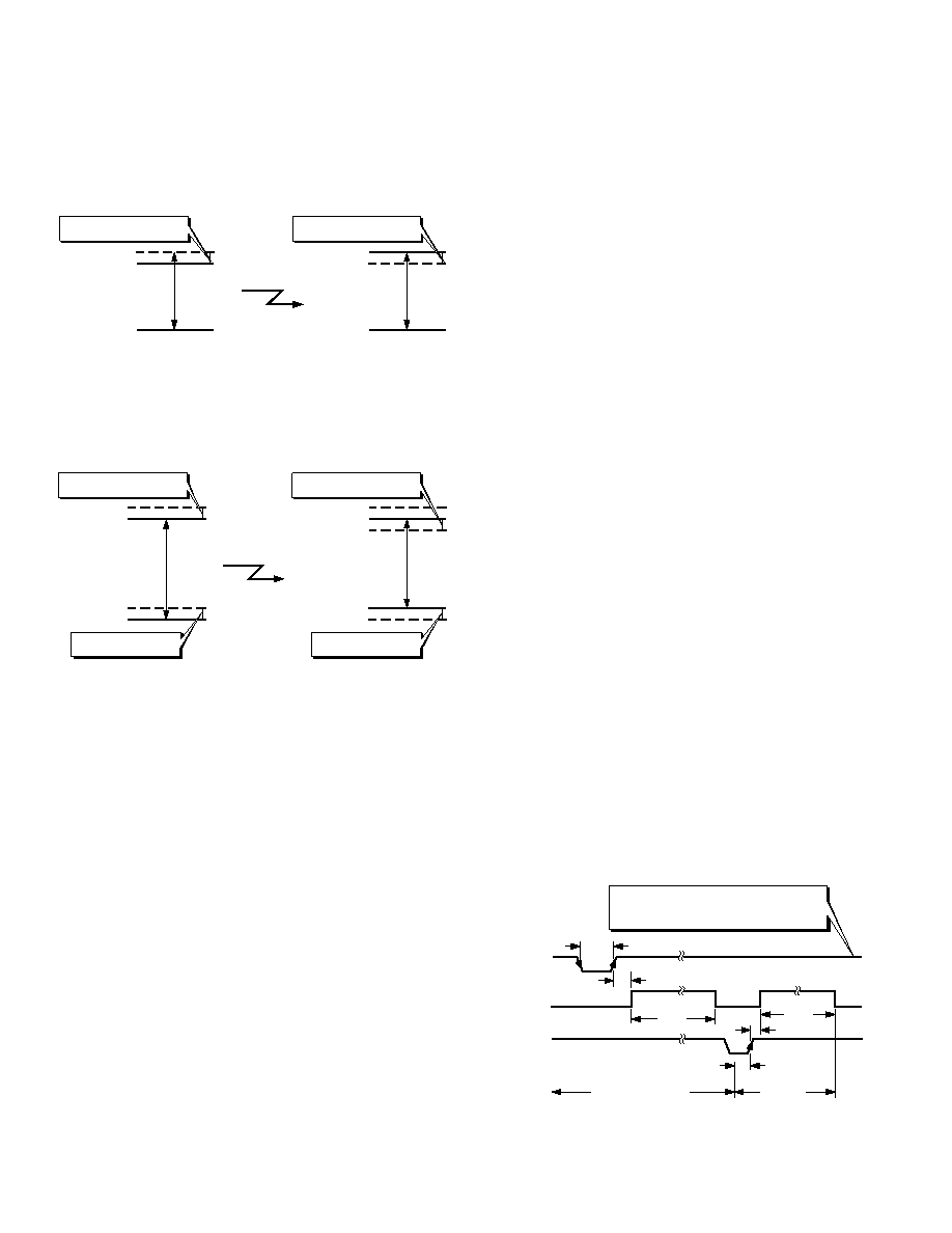
t1 = 100ns MIN, t14 = 50/90ns MIN 5V/3V,
t15 = 2.5 tCLKIN MAX, tCAL1 = 111114 tCLKIN,
tCAL2 = 13899 tCLKIN
t1
t15
tCAL1
tCAL2
t16
tSETUP
VSYSTEM FULL SCALE
VOFFSET
CAL (I/P)
BUSY (O/P)
CONVST (I/P)
AIN (I/P)
Figure 29. Timing Diagram for Full System Calibration
相关PDF资料 |
PDF描述 |
|---|---|
| MS3102R28-21SW | CONN RCPT 37POS BOX MNT W/SCKT |
| A5FBXAU | CONN PLUG CORD FMAL 5PIN BLK/AU |
| MS3102E28-21SY | CONN RCPT 37POS BOX MNT W/SCKT |
| 15282-18PG-321 | CONN JACK 18POS CABLE PIN |
| SP3082EEN-L/TR | IC TXRX RS485/RS422 ESD 8NSOIC |
相关代理商/技术参数 |
参数描述 |
|---|---|
| AD7858LAR | 制造商:Analog Devices 功能描述:ADC Single SAR 100ksps 12-bit Serial 24-Pin SOIC W |
| AD7858LAR3 | 制造商:AD 制造商全称:Analog Devices 功能描述:3 V to 5 V Single Supply, 200 kSPS 8-Channel, 12-Bit Sampling ADC |
| AD7858LAR-REEL | 制造商:Analog Devices 功能描述:ADC Single SAR 100ksps 12-bit Serial 24-Pin SOIC W T/R |
| AD7858LARS | 功能描述:IC ADC 12BIT 8CH SRL 24-SSOP RoHS:否 类别:集成电路 (IC) >> 数据采集 - 模数转换器 系列:- 标准包装:1,000 系列:- 位数:12 采样率(每秒):300k 数据接口:并联 转换器数目:1 功率耗散(最大):75mW 电压电源:单电源 工作温度:0°C ~ 70°C 安装类型:表面贴装 封装/外壳:24-SOIC(0.295",7.50mm 宽) 供应商设备封装:24-SOIC 包装:带卷 (TR) 输入数目和类型:1 个单端,单极;1 个单端,双极 |
| AD7858LARS3 | 制造商:AD 制造商全称:Analog Devices 功能描述:3 V to 5 V Single Supply, 200 kSPS 8-Channel, 12-Bit Sampling ADC |
发布紧急采购,3分钟左右您将得到回复。