- 您现在的位置:买卖IC网 > PDF目录10211 > AD7858LANZ (Analog Devices Inc)IC ADC 12BIT 8CHAN SRL 24DIP PDF资料下载
参数资料
| 型号: | AD7858LANZ |
| 厂商: | Analog Devices Inc |
| 文件页数: | 23/32页 |
| 文件大小: | 0K |
| 描述: | IC ADC 12BIT 8CHAN SRL 24DIP |
| 标准包装: | 15 |
| 位数: | 12 |
| 采样率(每秒): | 100k |
| 数据接口: | 8051,QSPI?,串行,SPI? µP |
| 转换器数目: | 2 |
| 功率耗散(最大): | 33mW |
| 电压电源: | 模拟和数字 |
| 工作温度: | -40°C ~ 85°C |
| 安装类型: | 通孔 |
| 封装/外壳: | 24-DIP(0.300",7.62mm) |
| 供应商设备封装: | 24-PDIP |
| 包装: | 管件 |
| 输入数目和类型: | 8 个单端,单极;4 个伪差分,单极 |
第1页第2页第3页第4页第5页第6页第7页第8页第9页第10页第11页第12页第13页第14页第15页第16页第17页第18页第19页第20页第21页第22页当前第23页第24页第25页第26页第27页第28页第29页第30页第31页第32页
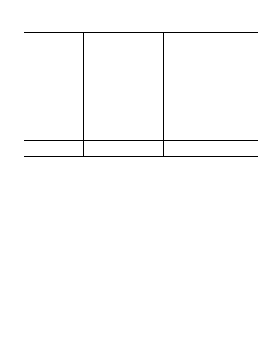
Parameter
A Version
1
B Version
1
Units
Test Conditions/Comments
DYNAMIC PERFORMANCE
AVDD, DVDD
+3.0/+5.5
V min/max
IDD
Normal Mode
5
6 (1.9)
mA max
AVDD = DVDD = 4.5 V to 5.5 V. Typically 4.5 mA (1.5)
5.5 (1.9)
mA max
AVDD = DVDD = 3.0 V to 3.6 V. Typically 4.0 mA (1.5 mA)
Sleep Mode
6
With External Clock On
10
A typ
Full Power-Down. Power Management Bits in Control
Register Set as PMGT1 = 1, PMGT0 = 0
400
A typ
Partial Power-Down. Power Management Bits in
Control Register Set as PMGT1 = 1, PMGT0 = 1
With External Clock Off
5
A max
Typically 1
A. Full Power-Down. Power Management Bits
in Control
Register Set as PMGT1 = 1, PMGT0 = 0
200
A typ
Partial Power-Down. Power Management Bits in Control
Register Set as PMGT1 = 1, PMGT0 = 1
Normal-Mode Power Dissipation
33 (10.5)
mW max
VDD = 5.5 V. Typically 25 mW (8); SLEEP = VDD
20 (6.85)
mW max
VDD = 3.6 V. Typically 15 mW (5.4); SLEEP = VDD
Sleep Mode Power Dissipation
With External Clock On
55
W typ
VDD = 5.5 V. SLEEP = 0 V
36
W typ
VDD = 3.6 V. SLEEP = 0 V
With External Clock Off
27.5
W max
VDD = 5.5 V. Typically 5.5
W; SLEEP = 0 V
18
W max
VDD = 3.6 V. Typically 3.6
W; SLEEP = 0 V
SYSTEM CALIBRATION
Offset Calibration Span
7
+0.05
× V
REF/–0.05
× V
REF
V max/min
Allowable Offset Voltage Span for Calibration
Gain Calibration Span
7
+1.025
× VREF/–0.975 × VREF
V max/min
Allowable Full-Scale Voltage Span for Calibration
NOTES
1Temperature ranges as follows: A, B Versions: –40
°C to +85°C. For L Versions, A and B Versions fCLKIN = 1 MHz over –40°C to +85°C temperature range,
B Version fCLKIN = 1.8 MHz over 0
°C to +70°C temperature range.
2Specifications apply after calibration.
3SNR calculation includes distortion and noise components.
4Sample tested @ +25
°C to ensure compliance.
5All digital inputs @ DGND except for
CONVST, SLEEP, CAL, and SYNC @ DV
DD. No load on the digital outputs. Analog inputs @ AGND.
6CLKIN @ DGND when external clock off. All digital inputs @ DGND except for
CONVST, SLEEP, CAL, and SYNC @ DV
DD. No load on the digital
outputs. Analog inputs @ AGND.
7The Offset and Gain Calibration Spans are defined as the range of offset and gain errors that the AD7858/AD7858L can calibrate. Note also that these are voltage
spans and are not absolute voltages ( i.e., the allowable system offset voltage presented at AIN(+) for the system offset error to be adjusted out will be AIN(–)
± 0.05 × V
REF, and the allowable system full-scale voltage applied between AIN(+) and AIN(–) for the system full-scale voltage error to be adjusted out will be
VREF
± 0.025 × V
REF). This is explained in more detail in the Calibration sect ion of the data sheet.
Specifications subject to change without notice.
AD7858/AD7858L
REV. B
–3–
相关PDF资料 |
PDF描述 |
|---|---|
| MS3102R28-21SW | CONN RCPT 37POS BOX MNT W/SCKT |
| A5FBXAU | CONN PLUG CORD FMAL 5PIN BLK/AU |
| MS3102E28-21SY | CONN RCPT 37POS BOX MNT W/SCKT |
| 15282-18PG-321 | CONN JACK 18POS CABLE PIN |
| SP3082EEN-L/TR | IC TXRX RS485/RS422 ESD 8NSOIC |
相关代理商/技术参数 |
参数描述 |
|---|---|
| AD7858LAR | 制造商:Analog Devices 功能描述:ADC Single SAR 100ksps 12-bit Serial 24-Pin SOIC W |
| AD7858LAR3 | 制造商:AD 制造商全称:Analog Devices 功能描述:3 V to 5 V Single Supply, 200 kSPS 8-Channel, 12-Bit Sampling ADC |
| AD7858LAR-REEL | 制造商:Analog Devices 功能描述:ADC Single SAR 100ksps 12-bit Serial 24-Pin SOIC W T/R |
| AD7858LARS | 功能描述:IC ADC 12BIT 8CH SRL 24-SSOP RoHS:否 类别:集成电路 (IC) >> 数据采集 - 模数转换器 系列:- 标准包装:1,000 系列:- 位数:12 采样率(每秒):300k 数据接口:并联 转换器数目:1 功率耗散(最大):75mW 电压电源:单电源 工作温度:0°C ~ 70°C 安装类型:表面贴装 封装/外壳:24-SOIC(0.295",7.50mm 宽) 供应商设备封装:24-SOIC 包装:带卷 (TR) 输入数目和类型:1 个单端,单极;1 个单端,双极 |
| AD7858LARS3 | 制造商:AD 制造商全称:Analog Devices 功能描述:3 V to 5 V Single Supply, 200 kSPS 8-Channel, 12-Bit Sampling ADC |
发布紧急采购,3分钟左右您将得到回复。