- 您现在的位置:买卖IC网 > PDF目录10211 > AD7858LANZ (Analog Devices Inc)IC ADC 12BIT 8CHAN SRL 24DIP PDF资料下载
参数资料
| 型号: | AD7858LANZ |
| 厂商: | Analog Devices Inc |
| 文件页数: | 7/32页 |
| 文件大小: | 0K |
| 描述: | IC ADC 12BIT 8CHAN SRL 24DIP |
| 标准包装: | 15 |
| 位数: | 12 |
| 采样率(每秒): | 100k |
| 数据接口: | 8051,QSPI?,串行,SPI? µP |
| 转换器数目: | 2 |
| 功率耗散(最大): | 33mW |
| 电压电源: | 模拟和数字 |
| 工作温度: | -40°C ~ 85°C |
| 安装类型: | 通孔 |
| 封装/外壳: | 24-DIP(0.300",7.62mm) |
| 供应商设备封装: | 24-PDIP |
| 包装: | 管件 |
| 输入数目和类型: | 8 个单端,单极;4 个伪差分,单极 |
第1页第2页第3页第4页第5页第6页当前第7页第8页第9页第10页第11页第12页第13页第14页第15页第16页第17页第18页第19页第20页第21页第22页第23页第24页第25页第26页第27页第28页第29页第30页第31页第32页
AD7858/AD7858L
REV. B
–15–
CIRCUIT INFORMATION
The AD7858/AD7858L is a fast, 12-bit single supply A/D con-
verter. The part requires an external 4 MHz/1.8 MHz master
clock (CLKIN), two CREF capacitors, a CONVST signal to start
conversion, and power supply decoupling capacitors. The part
provides the user with track/hold, on-chip reference, calibration
features, A/D converter, and serial interface logic functions on a
single chip. The A/D converter section of the AD7858/AD7858L
consists of a conventional successive-approximation converter
based around a capacitor DAC. The AD7858/AD7858L accepts
an analog input range of 0 to +VDD where the reference can be
tied to VDD. The reference input to the part is buffered on-chip.
A major advantage of the AD7858/AD7858L is that a conversion
can be initiated in software as well as applying a signal to the
CONVST pin. Another innovative feature of the AD7858/
AD7858L is self-calibration on power-up, which is initiated
having a capacitor from the
CAL pin to AGND, to give superior
dc accuracy. See Automatic Calibration on Power-Up section.
The part is available in a 24-pin SSOP package and this offers
the user considerable space-saving advantages over alternative
solutions. The AD7858L version typically consumes only
5.5 mW making it ideal for battery-powered applications.
CONVERTER DETAILS
The master clock for the part must be applied to the CLKIN
pin. Conversion is initiated on the AD7858/AD7858L by pulsing
the
CONVST input or by writing to the control register and
setting the CONVST bit to 1. On the rising edge of
CONVST
(or at the end of the control register write operation), the on-
chip track/hold goes from track to hold mode. The falling edge
of the CLKIN signal that follows the rising edge of the
CONVST
signal initiates the conversion, provided the rising edge of
CONVST occurs at least 10 ns typically before this CLKIN
edge. The conversion cycle will take 16.5 CLKIN periods from
this CLKIN falling edge. If the 10 ns setup time is not met, the
conversion will take 17.5 CLKIN periods. The maximum speci-
fied conversion time is 4.6
s for the AD7858 (18t
CLKIN,
CLKIN = 4 MHz) and 10
s for the AD7858L (18tCLKIN,
CLKIN = 1.8 MHz). When a conversion is completed, the
BUSY output goes low, and then the result of the conversion
can be read by accessing the data through the serial interface.
To obtain optimum performance from the part, the read opera-
tion should not occur during the conversion or 400 ns prior to
the next
CONVST rising edge. However, the maximum
throughput rates are achieved by reading/writing during conver-
sion, and reading/writing during conversion is likely to degrade
the Signal to (Noise + Distortion) by only 0.5 dBs. The AD7858
can operate at throughput rates up to 200 kHz, 100 kHz for the
AD7858L. For the AD7858 a conversion takes 18 CLKIN
periods; 2 CLKIN periods are needed for the acquisition time
giving a full cycle time of 5
s (= 200 kHz, CLKIN = 4 MHz).
For the AD7858L 100 kHz throughput can be obtained as
follows: the CLKIN and
CONVST signals are arranged to give
a conversion time of 16.5 CLKIN periods as described above,
1.5 CLKIN periods are allowed for the acquisition time. This
gives a full cycle time of 10
s (=100 kHz, CLKIN = 1.8 MHz).
When using the software conversion start for maximum through-
put the user must ensure the control register write operation
extends beyond the falling edge of BUSY. The falling edge of
BUSY resets the
CONVST bit to 0 and allows it to be repro-
grammed to 1 to start the next conversion.
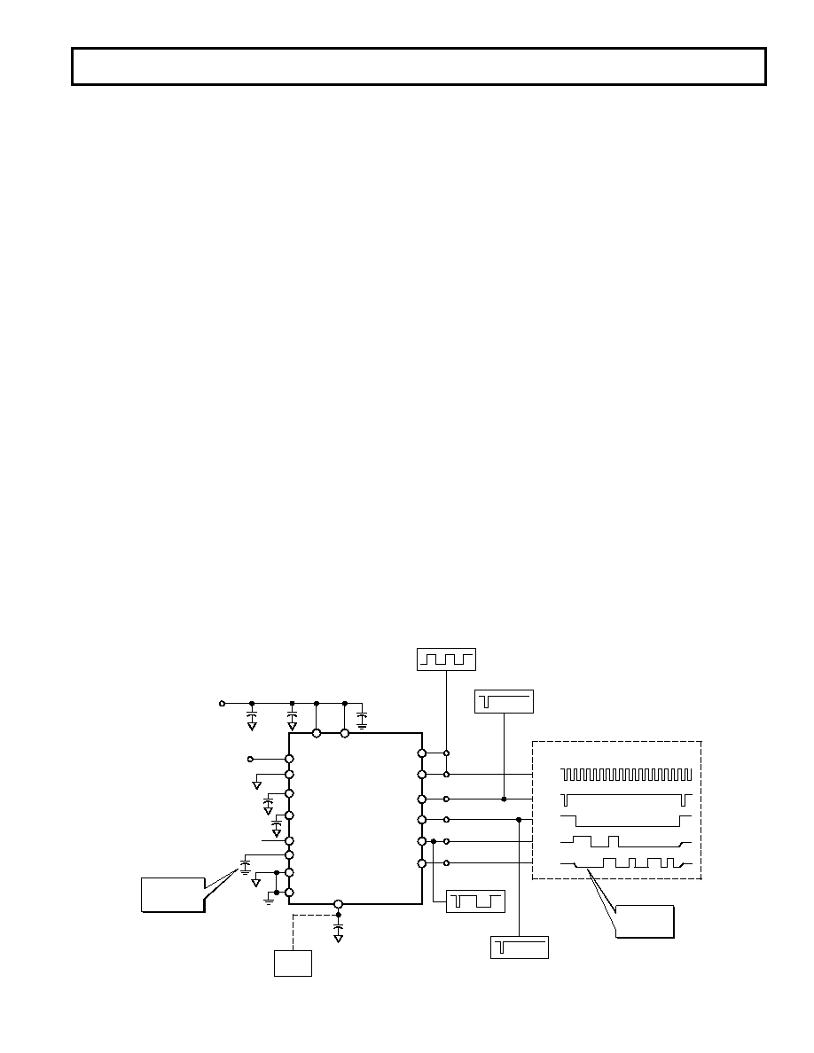
TYPICAL CONNECTION DIAGRAM
Figure 10 shows a typical connection diagram for the AD7858/
AD7858L. The AGND and the DGND pins are connected
together at the device for good noise suppression. The
CAL pin
has a 0.01
F capacitor to enable an automatic self-calibration
on power-up. The conversion result is output in a 16-bit word
with four leading zeros followed by the MSB of the 12-bit result.
Note that after the AVDD and DVDD power-up the part will
CH1
CH2
CH3
CH4
CH5
OSCILLOSCOPE
4 LEADING
ZEROS FOR
ADC DATA
AUTO CAL ON
POWER-UP
OPTIONAL
EXTERNAL
REFERENCE
AD780/
REF-192
4MHz/1.8MHz OSCILLATOR
MASTER CLOCK
INPUT
0.1 F
10 F
ANALOG SUPPLY
+3V TO +5V
0V TO 2.5V
INPUT
0.1 F
0.01 F
DVDD
0.01 F
0.1 F
INTERNAL/
EXTERNAL
REFERENCE
200kHz/100kHz PULSE GENERATOR
CONVERSION
START INPUT
SERIAL CLOCK
INPUT
FRAME SYNC INPUT
SERIAL DATA INPUT
SERIAL DATA
OUTPUT
DATA GENERATOR
PULSE GENERATOR
CLKIN
SCLK
CONVST
SYNC
DIN
DOUT
DGND
AGND
CAL
SLEEP
CREF2
CREF1
AIN(–)
AIN(+)
AVDD DVDD
AD7858/
AD7858L
Figure 10. Typical Circuit
相关PDF资料 |
PDF描述 |
|---|---|
| MS3102R28-21SW | CONN RCPT 37POS BOX MNT W/SCKT |
| A5FBXAU | CONN PLUG CORD FMAL 5PIN BLK/AU |
| MS3102E28-21SY | CONN RCPT 37POS BOX MNT W/SCKT |
| 15282-18PG-321 | CONN JACK 18POS CABLE PIN |
| SP3082EEN-L/TR | IC TXRX RS485/RS422 ESD 8NSOIC |
相关代理商/技术参数 |
参数描述 |
|---|---|
| AD7858LAR | 制造商:Analog Devices 功能描述:ADC Single SAR 100ksps 12-bit Serial 24-Pin SOIC W |
| AD7858LAR3 | 制造商:AD 制造商全称:Analog Devices 功能描述:3 V to 5 V Single Supply, 200 kSPS 8-Channel, 12-Bit Sampling ADC |
| AD7858LAR-REEL | 制造商:Analog Devices 功能描述:ADC Single SAR 100ksps 12-bit Serial 24-Pin SOIC W T/R |
| AD7858LARS | 功能描述:IC ADC 12BIT 8CH SRL 24-SSOP RoHS:否 类别:集成电路 (IC) >> 数据采集 - 模数转换器 系列:- 标准包装:1,000 系列:- 位数:12 采样率(每秒):300k 数据接口:并联 转换器数目:1 功率耗散(最大):75mW 电压电源:单电源 工作温度:0°C ~ 70°C 安装类型:表面贴装 封装/外壳:24-SOIC(0.295",7.50mm 宽) 供应商设备封装:24-SOIC 包装:带卷 (TR) 输入数目和类型:1 个单端,单极;1 个单端,双极 |
| AD7858LARS3 | 制造商:AD 制造商全称:Analog Devices 功能描述:3 V to 5 V Single Supply, 200 kSPS 8-Channel, 12-Bit Sampling ADC |
发布紧急采购,3分钟左右您将得到回复。