- 您现在的位置:买卖IC网 > PDF目录10211 > AD7858LANZ (Analog Devices Inc)IC ADC 12BIT 8CHAN SRL 24DIP PDF资料下载
参数资料
| 型号: | AD7858LANZ |
| 厂商: | Analog Devices Inc |
| 文件页数: | 22/32页 |
| 文件大小: | 0K |
| 描述: | IC ADC 12BIT 8CHAN SRL 24DIP |
| 标准包装: | 15 |
| 位数: | 12 |
| 采样率(每秒): | 100k |
| 数据接口: | 8051,QSPI?,串行,SPI? µP |
| 转换器数目: | 2 |
| 功率耗散(最大): | 33mW |
| 电压电源: | 模拟和数字 |
| 工作温度: | -40°C ~ 85°C |
| 安装类型: | 通孔 |
| 封装/外壳: | 24-DIP(0.300",7.62mm) |
| 供应商设备封装: | 24-PDIP |
| 包装: | 管件 |
| 输入数目和类型: | 8 个单端,单极;4 个伪差分,单极 |
第1页第2页第3页第4页第5页第6页第7页第8页第9页第10页第11页第12页第13页第14页第15页第16页第17页第18页第19页第20页第21页当前第22页第23页第24页第25页第26页第27页第28页第29页第30页第31页第32页
AD7858/AD7858L
REV. B
–29–
A typical sequence of events would be to write to the control
register via the DIN line setting a conversion start and at the
same time reading data from the previous conversion on the
DOUT line (both the read and write operations would each be
two 8-bit operations, one 16-bit operation for the 68HC16),
wait for the conversion to be finished (= 4.6
s for AD7858
with 4 MHz CLKIN), and then repeat the sequence. The maxi-
mum serial frequency will be determined by the data access and
hold times of the
Controllers and the AD7858/AD7858L.
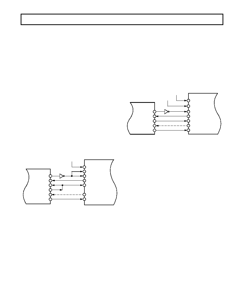
AD7858/AD7858L to ADSP-21xx Interface
Figure 39 shows the AD7858/AD7858L interface to the ADSP-
21xx. The ADSP-21xx is the master and the AD7858/AD7858L
is the slave. The AD7858/AD7858L is in Interface Mode 2.
For the ADSP-21xx the bits in the serial port control register
should be set up as TFSR = RFSR = 1 (need a frame sync for
every transfer), SLEN = 15 (16-bit word length), TFSW =
RFSW = 1 (alternate framing mode for transmit and receive
operations), INVRFS = INVTFS = 1 (active low RFS and
TFS), IRFS = 0, ITFS = 1 (External RFS and internal TFS),
and ISCLK = 1 (internal serial clock). The CLKIN and
CONVST signals can be supplied from the ADSP-21xx or
from an external source. The serial clock from the ADSP-21xx
must be inverted before the SCLK pin of the AD7858/AD7858L.
This SCLK could also be used to drive the CLKIN input of the
AD7858/AD7858L. The BUSY signal indicates when the con-
version is finished and may not be required. The data access
and hold times of the ADSP-21xx and the AD7858/AD7858L
allow for a serial clock of 4 MHz/1.8 MHz at 5 V and 3.3 MHz/
1.8 MHz at 3 V supplies.
ADSP-21xx
CONVST
CLKIN
DOUT
DIN
SYNC
OPTIONAL
4MHz/1.8MHz
BUSY
IRQ
MASTER
SLAVE
TFS
DT
SCK
SCLK
RFS
DR
OPTIONAL
AD7858/AD7858L
Figure 39. ADSP-21xx Interface
AD7858/AD7858L to DSP56000/1/2/L002 Interface
Figure 40 shows the AD7858/AD7858L to DSP56000/1/2/
L002 interface. Here the DSP5600x is the master and the
AD7858 is the slave. The AD7858/AD7858L is in Interface
Mode 2. The DSP56L002 is used when the AD7858/AD7858L
is being operated at 3 V. The setting of the bits in the registers
of the DSP5600x would be for synchronous operation (SYN =
1), internal frame sync (SCD2 = 1), gated internal clock (GCK
= 1, SCKD = 1), 16-bit word length (WL1 = 1, WL0 = 0). Since
a gated clock is used here the SCLK cannot be tied to the CLKIN
of the AD7858/AD7858L. The SCLK from the DSP5600x
must be inverted before it is applied to the AD7858/AD7858L.
Again the data access and hold times of the DSP5600x and
the AD7858/AD7858L allows for a SCLK of 4 MHz/1.8 MHz.
DSP56000/1/2/L002
SRD
CONVST
CLKIN
SCLK
DIN
SYNC
OPTIONAL
BUSY
IRQ
MASTER
SLAVE
OPTIONAL
DOUT
SC2
STD
SCK
4MHz/1.8MHz
AD7858/AD7858L
Figure 40. DSP56000/1/2 Interface
相关PDF资料 |
PDF描述 |
|---|---|
| MS3102R28-21SW | CONN RCPT 37POS BOX MNT W/SCKT |
| A5FBXAU | CONN PLUG CORD FMAL 5PIN BLK/AU |
| MS3102E28-21SY | CONN RCPT 37POS BOX MNT W/SCKT |
| 15282-18PG-321 | CONN JACK 18POS CABLE PIN |
| SP3082EEN-L/TR | IC TXRX RS485/RS422 ESD 8NSOIC |
相关代理商/技术参数 |
参数描述 |
|---|---|
| AD7858LAR | 制造商:Analog Devices 功能描述:ADC Single SAR 100ksps 12-bit Serial 24-Pin SOIC W |
| AD7858LAR3 | 制造商:AD 制造商全称:Analog Devices 功能描述:3 V to 5 V Single Supply, 200 kSPS 8-Channel, 12-Bit Sampling ADC |
| AD7858LAR-REEL | 制造商:Analog Devices 功能描述:ADC Single SAR 100ksps 12-bit Serial 24-Pin SOIC W T/R |
| AD7858LARS | 功能描述:IC ADC 12BIT 8CH SRL 24-SSOP RoHS:否 类别:集成电路 (IC) >> 数据采集 - 模数转换器 系列:- 标准包装:1,000 系列:- 位数:12 采样率(每秒):300k 数据接口:并联 转换器数目:1 功率耗散(最大):75mW 电压电源:单电源 工作温度:0°C ~ 70°C 安装类型:表面贴装 封装/外壳:24-SOIC(0.295",7.50mm 宽) 供应商设备封装:24-SOIC 包装:带卷 (TR) 输入数目和类型:1 个单端,单极;1 个单端,双极 |
| AD7858LARS3 | 制造商:AD 制造商全称:Analog Devices 功能描述:3 V to 5 V Single Supply, 200 kSPS 8-Channel, 12-Bit Sampling ADC |
发布紧急采购,3分钟左右您将得到回复。