- 您现在的位置:买卖IC网 > PDF目录10047 > AD7872ANZ (Analog Devices Inc)IC ADC 14BIT SAMPLING 16DIP PDF资料下载
参数资料
| 型号: | AD7872ANZ |
| 厂商: | Analog Devices Inc |
| 文件页数: | 14/16页 |
| 文件大小: | 0K |
| 描述: | IC ADC 14BIT SAMPLING 16DIP |
| 标准包装: | 1 |
| 位数: | 14 |
| 采样率(每秒): | 83k |
| 数据接口: | 串行 |
| 转换器数目: | 1 |
| 功率耗散(最大): | 95mW |
| 电压电源: | 双 ± |
| 工作温度: | -40°C ~ 85°C |
| 安装类型: | 通孔 |
| 封装/外壳: | 16-DIP(0.300",7.62mm) |
| 供应商设备封装: | 16-PDIP |
| 包装: | 管件 |
| 输入数目和类型: | 1 个单端,双极 |
AD7871/AD7872
–7–
REV. D
Gain error can be adjusted at either the first code transition
(ADC negative full scale) or the last code transition (ADC posi-
tive full scale). The trim procedures for both cases are as follows
(see Figure 6).
Positive Full-Scale Adjust
Apply a voltage of 2.9995 V (FS/2 –3/2 LSBs) at V1 and adjust
R2 until the ADC output code flickers between 01 1111 1111
1110 and 01 1111 1111 1111.
Negative Full-Scale Adjust
Apply a voltage of –2.9998 V (–FS/2 + 1/2 LSB) at V1 and ad-
just R2 until the ADC output code flickers between 10 0000
0000 0000 and 10 0000 0000 0001.
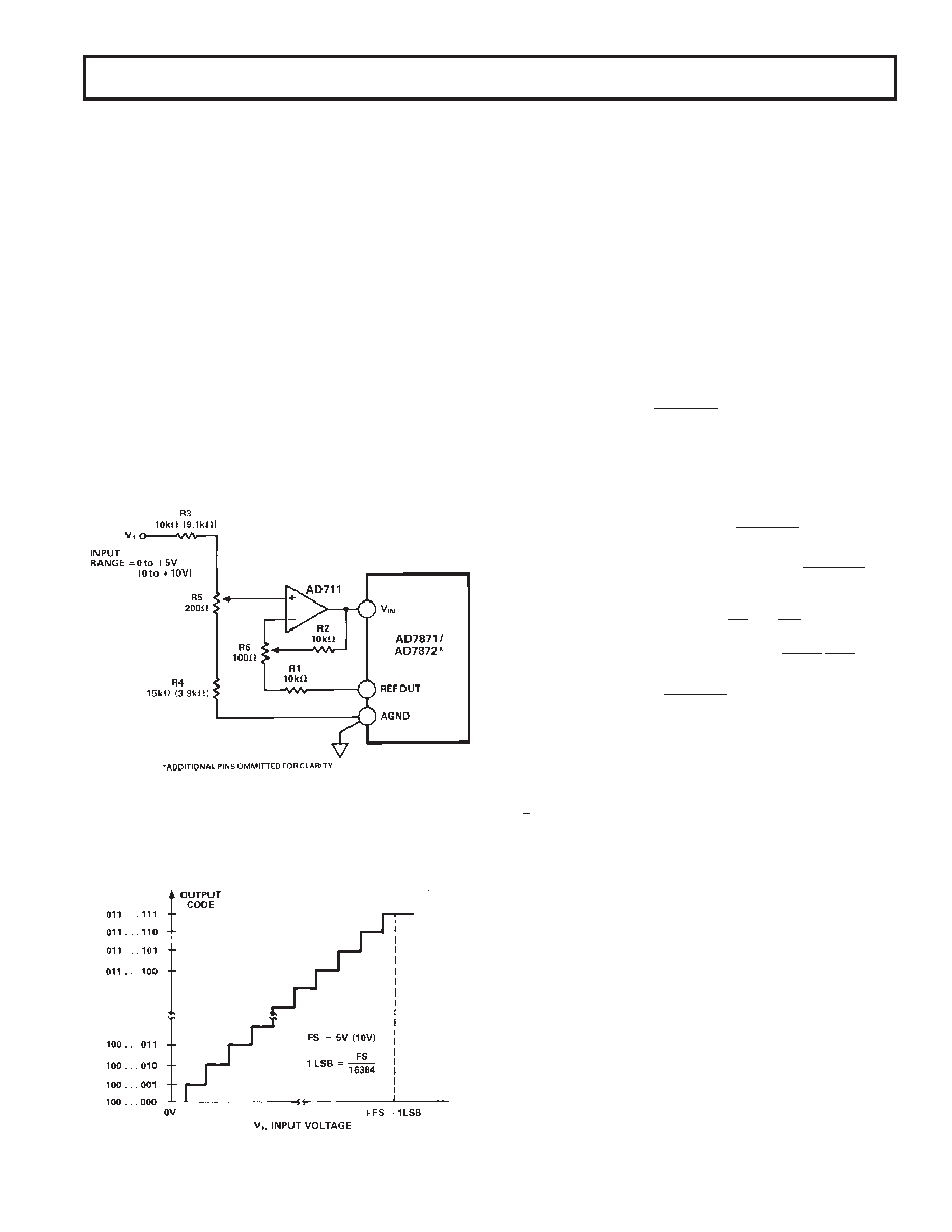
UNIPOLAR OPERATION
A typical unipolar circuit is shown in Figure 7. The AD7871/
AD7872 REF OUT is used to offset the analog input by 3 V.
The analog input range is determined by the ratio of R3 to R4.
The minimum range with which the circuit will work is 0 to
+3 V. The resistor values are given in Figure 7 for input ranges
of 0 to +5 V and 0 to +10 V. R5 and R6 are included for offset
and full scale adjust only and should be omitted if adjustment is
not required.
Figure 7. Unipolar Circuit
The ideal input/output transfer function is shown in Figure 8.
The output can be converted to straight binary by inverting the
MSB.
Figure 8. Unipolar Transfer Function
UNIPOLAR OFFSET AND FULL-SCALE ADJUSTMENT
When absolute accuracy is required, offset and full-scale error
can be adjusted to zero. Offset must be adjusted before full-
scale. This is achieved by applying an input voltage of 1/2 LSB
to V1 and adjust R6 until the ADC output code flickers between
10 0000 0000 0000 and 10 0000 0000 0001. For full-scale
adjustment apply an input voltage of (FS –3/2 LSBs) to V1 and
adjust R5 until the output code flickers between 01 1111 1111
1110 and 01 1111 1111 1111.
TIMING AND CONTROL
The conversion time for both external and internal clocks can
vary from 19 to 20 rising clock edges depending on the conver-
sion start to ADC clock synchronization. If a conversion is initi-
ated within 30 ns prior to a rising edge of the ADC clock, the
conversion time will consist of 20 rising clock edges.
There are two basic operating modes for the AD7871. In the
first mode (Mode 1) the
CONVST line is used to start conver-
sion and drive the track/hold into its hold mode. At the end of
conversion, the track/hold returns to its tracking mode. It is
principally intended for digital signal processing and other
applications where precise sampling in time is required. In these
applications, it is important that the signal sampling occurs at
exactly equal intervals to minimize errors due to sampling un-
certainty or jitter. For these cases, the
CONVST line is driven
by a timer or some precise clock source.
The second mode is achieved by hard-wiring the
CONVST line
low. This mode (Mode 2) is intended for use in systems where
the microprocessor has total control of the ADC, both initiating
the conversion and reading the data.
CS and RD start conver-
sion, and the microprocessor will normally be driven into a
WAIT state for the duration of conversion by
BUSY/INT.
The AD7872 has one operating mode only. This is Mode 1, de-
scribed above, which uses
CONVST to start conversion.
DATA OUTPUT FORMATS
The AD7871 offers a choice of three data output formats, one
serial and two parallel. The parallel data formats include a single
14-bit parallel word for 16-bit data buses and a two-byte format
for 8-bit data buses. The data format is controlled by the
14/
8/CLK input. A logic high on this pin selects the 14-bit par-
allel output format only. A logic low or –5 V applied to this pin
allows the user access to either serial or byte formatted data.
Three of the pins previously assigned to the four MSBs in paral-
lel form are now used for serial communications while the
fourth pin becomes a control input for the byte-formatted data.
The three possible data output formats can be selected in either
of the modes of operation.
The AD7872 is a serial output device only. The serial data for-
mat is exactly the same as the AD7871.
Parallel Output Format
The two parallel formats available on the AD7871 are a 14-bit
wide data word and a 2-byte data word. In the first, all 14 bits
of data are available at the same time on DB13 (MSB) through
DB0 (LSB). In the second, two reads are required to access the
data. When this data format is selected, the DB13/HBEN pin
assumes the HBEN function. HBEN selects which byte of data
is to be read from the AD7871. When HBEN is low, the lower
eight bits of data are placed on the data bus during a read opera-
tion; with HBEN high, the upper six bits of the 14-bit word are
相关PDF资料 |
PDF描述 |
|---|---|
| AD676KNZ | IC ADC 16BIT 100KSPS 28-DIP |
| MS3106E28-21PW | CONN PLUG 37POS STRAIGHT W/PINS |
| MS3106E20-29SZ | CONN PLUG 17POS STRAIGHT W/SCKT |
| MS27473T10C99S | CONN PLUG 7POS STRAIGHT W/SCKT |
| IDT72V801L20PF | IC SYNC FIFO 256X9 20NS 64QFP |
相关代理商/技术参数 |
参数描述 |
|---|---|
| AD7872AQ | 制造商:未知厂家 制造商全称:未知厂家 功能描述:Analog-to-Digital Converter, 14-Bit |
| AD7872BQ | 制造商:未知厂家 制造商全称:未知厂家 功能描述:Analog-to-Digital Converter, 14-Bit |
| AD7872BR | 功能描述:IC ADC 14BIT SAMPLING 16-SOIC RoHS:否 类别:集成电路 (IC) >> 数据采集 - 模数转换器 系列:- 标准包装:1 系列:- 位数:14 采样率(每秒):83k 数据接口:串行,并联 转换器数目:1 功率耗散(最大):95mW 电压电源:双 ± 工作温度:0°C ~ 70°C 安装类型:通孔 封装/外壳:28-DIP(0.600",15.24mm) 供应商设备封装:28-PDIP 包装:管件 输入数目和类型:1 个单端,双极 |
| AD7872BR-REEL | 功能描述:IC ADC 14BIT SAMPLING 16-SOIC RoHS:否 类别:集成电路 (IC) >> 数据采集 - 模数转换器 系列:- 标准包装:1 系列:- 位数:14 采样率(每秒):83k 数据接口:串行,并联 转换器数目:1 功率耗散(最大):95mW 电压电源:双 ± 工作温度:0°C ~ 70°C 安装类型:通孔 封装/外壳:28-DIP(0.600",15.24mm) 供应商设备封装:28-PDIP 包装:管件 输入数目和类型:1 个单端,双极 |
| AD7872BRZ | 功能描述:IC ADC 14BIT SAMPLING 16SOIC RoHS:是 类别:集成电路 (IC) >> 数据采集 - 模数转换器 系列:- 标准包装:1 系列:- 位数:14 采样率(每秒):83k 数据接口:串行,并联 转换器数目:1 功率耗散(最大):95mW 电压电源:双 ± 工作温度:0°C ~ 70°C 安装类型:通孔 封装/外壳:28-DIP(0.600",15.24mm) 供应商设备封装:28-PDIP 包装:管件 输入数目和类型:1 个单端,双极 |
发布紧急采购,3分钟左右您将得到回复。