- 您现在的位置:买卖IC网 > PDF目录10047 > AD7872ANZ (Analog Devices Inc)IC ADC 14BIT SAMPLING 16DIP PDF资料下载
参数资料
| 型号: | AD7872ANZ |
| 厂商: | Analog Devices Inc |
| 文件页数: | 5/16页 |
| 文件大小: | 0K |
| 描述: | IC ADC 14BIT SAMPLING 16DIP |
| 标准包装: | 1 |
| 位数: | 14 |
| 采样率(每秒): | 83k |
| 数据接口: | 串行 |
| 转换器数目: | 1 |
| 功率耗散(最大): | 95mW |
| 电压电源: | 双 ± |
| 工作温度: | -40°C ~ 85°C |
| 安装类型: | 通孔 |
| 封装/外壳: | 16-DIP(0.300",7.62mm) |
| 供应商设备封装: | 16-PDIP |
| 包装: | 管件 |
| 输入数目和类型: | 1 个单端,双极 |
AD7871/AD7872
–13–
REV. D
LAYOUT HINTS
Ensure that the layout for the printed circuit board has the digi-
tal and analog signal lines separated as much as possible. Take
care not to run a digital track alongside an analog signal track.
Guard (screen) the analog input with AGND.
Establish a single point analog ground (star ground) separate
from the logic system ground at the AD7871/AD7872 AGND
pin or as close as possible to the AD7871/AD7872. Connect all
other grounds and the AD7871/AD7872 DGND to this single
analog ground point. Do not connect any other digital grounds
to this analog ground point.
Low impedance analog and digital power supply common re-
turns are essential to low noise operation of the ADC, so make
the foil width for these tracks as wide as possible. The use of
ground planes minimizes impedance paths and also guards the
analog circuitry from digital noise. The circuit layout of Figures
26 and 27 have both analog and digital ground planes that are
kept separated and joined together only at the AD7871/AD7872
AGND pin.
NOISE
Keep the input signal leads to VIN and signal return leads from
AGND as short as possible to minimize input noise coupling. In
applications where this is not possible, use a shielded cable be-
tween the source and the ADC. Reduce the ground circuit im-
pedance as much as possible since any potential difference in
grounds between the signal source and the ADC appears as an
error voltage in series with the input signal.
DATA ACQUISITION BOARD
Figure 24 shows the AD7871/AD7872 in a data acquisition cir-
cuit. The corresponding printed circuit board (PCB) layout has
three interface ports: one serial and two parallel. Note that the
AD7871/AD7872 serial lines are buffered by a 74HC244. This
allows long lines with large capacitive loads to be driven. One of
the parallel ports is directly compatible with the ADSP-2100
evaluation board expansion connector.
The only additional component required for a full data acquisi-
tion system is an anti-aliasing filter. There is a component grid
provided near the analog input on the PCB, which may be used
for such a filter or any other input conditioning circuitry. To fa-
cilitate this option, there is a shorting plug (labelled LK1 on the
PCB) on the analog input track. If this shorting plug is used, the
analog input connects to the buffer amplifier driving the AD7871/
AD7872; if this shorting plug is omitted, a wire link can be used to
connect the analog input to the PCB component grid.
INTERFACE CONNECTIONS
There are two parallel connectors labeled SKT4 and SKT6,
and one serial connector labeled SKT5. A shorting plug option
(LK3 in Figure 24) configures the ADC for the appropriate
interface.
SKT6 is a 96-contact (3-row) Eurocard connector that is directly
compatible with the ADSP-2100 Evaluation Board Prototype
Expansion Connector. The expansion connector on the
ADSP-2100 has eight decoded chip enable outputs labeled
ECE1 to ECE8. ECE6 is used to drive the AD7871
CS input
on the board. To avoid selecting the onboard RAM sockets at
the same time, LK6 on the ADSP-2100 board must be removed.
In addition, the ADSP-2100 expansion connector has four in-
terrupts labelled EIRQ0 to EIRQ3. The AD7871
BUSY/INT
output connects to EIRQ0. There is a single wait state generator
connected to EDMACK to allow the AD7871 to interface to the
faster versions of the ADSP-2100.
SKT4 is a 26-way (2-row) IDC connector. This contains the
same signal contacts as SKT6 except for EDMACK, which is
connected to SKT6 only. It also contains decoded R/
W and
STRB inputs necessary for TMS32020 interfacing.
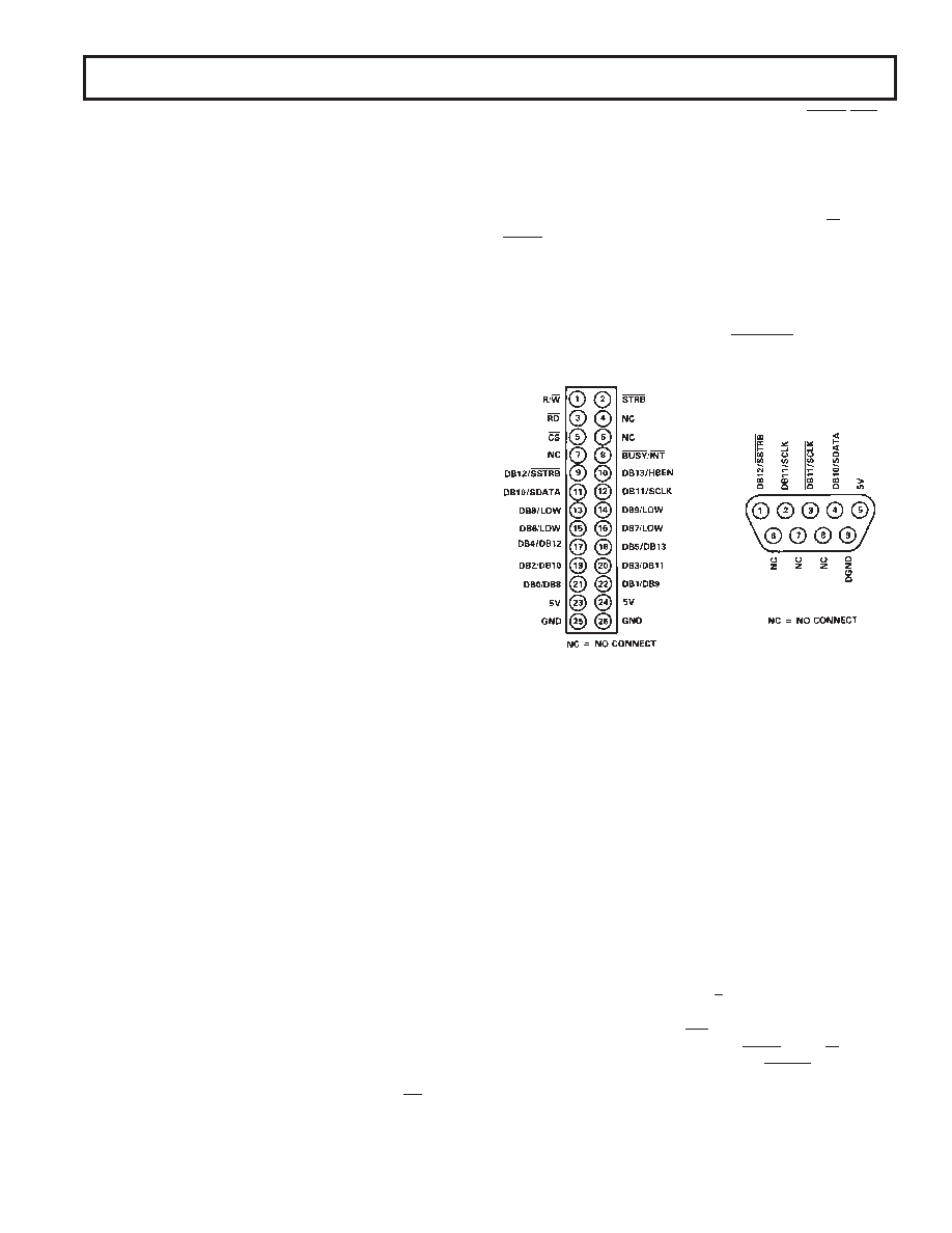
SKT5 is a 5-way D-type connector meant for serial interfacing
only. An inverted DB11/SCLK output is also provided on this
connector for systems that accept data on a rising clock edge.
SKT1, SKT2 and SKT3 are three BNC connectors providing
connections for the analog input, the
CONVST input and an
external clock.
Figure 22. SKT4 Pinout
Figure 23. SKT5 Pinout
POWER SUPPLY CONNECTIONS
The PCB requires two analog power supplies and one 5 V logic
supply. The analog supplies are labelled V+ and V–, and the
range for both supplies is 12 V to 15 V. Connection to the 5 V
digital supply is made through any of the connectors SKT4 to
SKT6. The
±5 V supply required by the AD7871 and AD7872
is generated from voltage regulators on the V+ and V– power
supplies input (IC6 and IC7 in Figure 24).
SHORTING PLUG OPTIONS
There are seven shorting plug options which must be set before
using the board. These are outlined below:
LK1
Connects the analog input to a buffer amplifier. The
analog input may also be connected to a component
grid for signal conditioning.
LK2
Selects either the AD7871/AD7872 internal clock or
an external clock source.
LK3
Configures the AD7871 14/
8/CLK input for the
appropriate serial or parallel interface.
LK4
Connects the AD7871
RD input directly to the two par-
allel connectors or to a decoded
STRB and R/W input.
LK5
Connects the pull-up resistor R3 to
SSTRB.
LK6
Connects the pull-up resistor R4 to SCLK.
LK7
Connects the pull-up resistor R5 to SDATA.
Note that LK5 to LK7 should be removed for parallel interfacing.
相关PDF资料 |
PDF描述 |
|---|---|
| AD676KNZ | IC ADC 16BIT 100KSPS 28-DIP |
| MS3106E28-21PW | CONN PLUG 37POS STRAIGHT W/PINS |
| MS3106E20-29SZ | CONN PLUG 17POS STRAIGHT W/SCKT |
| MS27473T10C99S | CONN PLUG 7POS STRAIGHT W/SCKT |
| IDT72V801L20PF | IC SYNC FIFO 256X9 20NS 64QFP |
相关代理商/技术参数 |
参数描述 |
|---|---|
| AD7872AQ | 制造商:未知厂家 制造商全称:未知厂家 功能描述:Analog-to-Digital Converter, 14-Bit |
| AD7872BQ | 制造商:未知厂家 制造商全称:未知厂家 功能描述:Analog-to-Digital Converter, 14-Bit |
| AD7872BR | 功能描述:IC ADC 14BIT SAMPLING 16-SOIC RoHS:否 类别:集成电路 (IC) >> 数据采集 - 模数转换器 系列:- 标准包装:1 系列:- 位数:14 采样率(每秒):83k 数据接口:串行,并联 转换器数目:1 功率耗散(最大):95mW 电压电源:双 ± 工作温度:0°C ~ 70°C 安装类型:通孔 封装/外壳:28-DIP(0.600",15.24mm) 供应商设备封装:28-PDIP 包装:管件 输入数目和类型:1 个单端,双极 |
| AD7872BR-REEL | 功能描述:IC ADC 14BIT SAMPLING 16-SOIC RoHS:否 类别:集成电路 (IC) >> 数据采集 - 模数转换器 系列:- 标准包装:1 系列:- 位数:14 采样率(每秒):83k 数据接口:串行,并联 转换器数目:1 功率耗散(最大):95mW 电压电源:双 ± 工作温度:0°C ~ 70°C 安装类型:通孔 封装/外壳:28-DIP(0.600",15.24mm) 供应商设备封装:28-PDIP 包装:管件 输入数目和类型:1 个单端,双极 |
| AD7872BRZ | 功能描述:IC ADC 14BIT SAMPLING 16SOIC RoHS:是 类别:集成电路 (IC) >> 数据采集 - 模数转换器 系列:- 标准包装:1 系列:- 位数:14 采样率(每秒):83k 数据接口:串行,并联 转换器数目:1 功率耗散(最大):95mW 电压电源:双 ± 工作温度:0°C ~ 70°C 安装类型:通孔 封装/外壳:28-DIP(0.600",15.24mm) 供应商设备封装:28-PDIP 包装:管件 输入数目和类型:1 个单端,双极 |
发布紧急采购,3分钟左右您将得到回复。