- 您现在的位置:买卖IC网 > PDF目录10047 > AD7872ANZ (Analog Devices Inc)IC ADC 14BIT SAMPLING 16DIP PDF资料下载
参数资料
| 型号: | AD7872ANZ |
| 厂商: | Analog Devices Inc |
| 文件页数: | 15/16页 |
| 文件大小: | 0K |
| 描述: | IC ADC 14BIT SAMPLING 16DIP |
| 标准包装: | 1 |
| 位数: | 14 |
| 采样率(每秒): | 83k |
| 数据接口: | 串行 |
| 转换器数目: | 1 |
| 功率耗散(最大): | 95mW |
| 电压电源: | 双 ± |
| 工作温度: | -40°C ~ 85°C |
| 安装类型: | 通孔 |
| 封装/外壳: | 16-DIP(0.300",7.62mm) |
| 供应商设备封装: | 16-PDIP |
| 包装: | 管件 |
| 输入数目和类型: | 1 个单端,双极 |
AD7871/AD7872
–8–
REV. D
placed on the data bus. These six bits are right justified and
thereby occupy the lower six bits of the byte while the upper two
bits are zeros.
Serial Output Format
Serial data is available on the AD7871 when the 14/
8/CLK
input is at 0 V or –5 V and in this case the DB12/
SSTRB,
DB11/SCLK and DB10/SDATA pins assume their serial func-
tions. The AD7872 is a serial output device only. The serial
function on both devices is identical. Serial data is available dur-
ing conversion with a word length of 16 bits; two leading zeros,
followed by the 14-bit conversion result starting with the MSB.
The data is synchronized to the serial clock output (SCLK) and
is framed by the serial strobe (
SSTRB). Data is clocked out on a
low to high transition of the serial clock and is valid on the fall-
ing edge of this clock while the
SSTRB output is low. SSTRB
goes low at the start of conversion and the first serial data bit
(which is the first leading zero) is valid on the first falling edge
of SCLK. All the serial lines are open-drain outputs and require
external pull-up resistors.
The serial clock out is derived from the ADC master clock
source which may be internal or external. Normally, SCLK is
required during the serial transmission only. In these cases it
can be shut down (i.e., placed into three-state) at the end of
conversion to allow multiple ADCs to share a common serial
bus. However, some serial systems (e.g., TMS32020) require a
serial clock that runs continuously. Both options are available
on the AD7871 and AD7872. With the 14/
8/CLK input on the
AD7871 at –5 V, the serial clock (SCLK) runs continuously;
when 14/
8/CLK is at 0 V, SCLK goes into three-state at the end
of transmission. The CONTROL pin on the AD7872 performs
the same function. When this is at 0 V, SCLK is noncontinuous
and when it is at –5 V, SCLK is continuous.
The SCLK, SDATA and
SSTRB lines are open-drain outputs.
If these are required to drive capacitive loads in excess of 35 pF,
buffering is recommended.
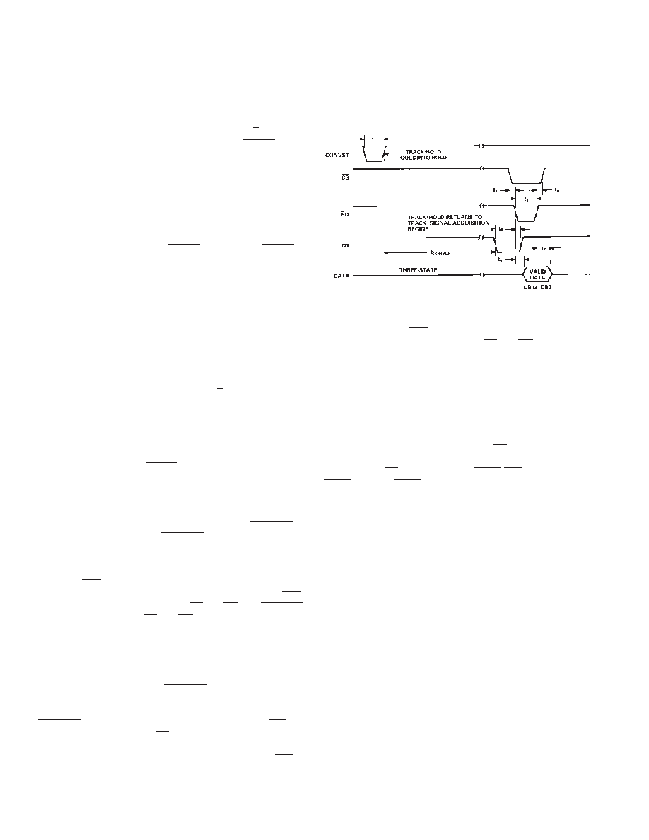
MODE 1 INTERFACE
Conversion is initiated by a low going pulse on the
CONVST
input. The rising edge of this
CONVST pulse starts conversion
and drives the track/hold amplifier into its hold mode. The
BUSY/INT status output assumes its INT function in this
mode.
INT is normally high and goes low at the end of conver-
sion. This
INT line can be used to interrupt the microprocessor.
A read operation to the AD7871 accesses the data and the
INT
line is reset high on the falling edge of
CS and RD. The CONVST
input must be high when
CS and RD are brought low for the
AD7871 to operate correctly in this mode. It is important, espe-
cially in systems where the conversion start (
CONVST) pulse is
asynchronous to the microprocessor, to ensure that a parallel or
byte data read is not attempted during a conversion. Trying to
read data during a conversion can cause errors to the conversion
in progress. Avoid pulsing the
CONVST line a second time be-
fore conversion end since it can cause errors in the conversion
result. In applications where precise sampling is not critical, the
CONVST pulse can be generated from microprocessor WR line
OR-gated with the AD7871
CS input. In some applications, de-
pending on power supply turn-on time, the AD7871/AD7872
may perform a conversion on power-up. In this case, the
INT
line on the AD7871 will power up low, and a dummy read to
the device will be required to reset the
INT line before starting
conversion.
Figure 9 shows the Mode 1 timing diagram for a 14-bit parallel
data output format (14/
8/CLK = +5 V). A read to the AD7871
at the end of conversion accesses all 14 bits of data at the same
time. Serial data is not available for this data output format.
Figure 9. Mode 1 Timing Diagram, 14-Bit Parallel Read
The Mode 1 function timing diagram for byte and serial data is
shown in Figure 10.
INT goes low at the end of conversion and
is reset high by the first falling edge of
CS and RD. This first
read at the end of conversion can either access the low byte or
high byte of data depending on the status of HBEN (Figure 10
shows low byte for example only). The diagram shows both the
SCLK output going into three-state at the end of transmission
and a continuously running clock (dashed line).
MODE 2 INTERFACE
The second interface mode is achieved by hard-wiring
CONVST
low and conversion is initiated by taking
CS low while HBEN is
low. The track/hold amplifier goes into the hold mode on the
falling edge of
CS. In this mode the BUSY/INT pin assumes its
BUSY function. BUSY goes low at the start of conversion, stays
low during the conversion and returns high when the conversion
is complete. It is normally used in parallel interfaces to drive the
microprocessor into a WAIT state for the duration of conversion.
Figure 11 shows the Mode 2 timing diagram for the 14-bit paral-
lel data output format (14/
8/CLK = +5 V). In this case the ADC
behaves like slow memory. The major advantage of this interface
is that it allows the microprocessor to start conversion, WAIT
and then read data with a single READ instruction. The user
does not have to worry about servicing interrupts or ensuring
that software delays are long enough to avoid the reading during
conversion.
The Mode 2 timing diagram for byte and serial data is shown in
Figure 12. For 2-byte data read, the lower byte (DB0–DB7) has
to be accessed first since HBEN must be low to start con-ver-
sion. The ADC behaves like slow memory for this first read, but
the second read to access the upper byte of data is a normal read.
Operation to the serial functions is identical between Mode 1
and Mode 2. Once again, the timing diagram of Figure 12 shows
SCLK going into three-state or running continuously (dashed
line).
相关PDF资料 |
PDF描述 |
|---|---|
| AD676KNZ | IC ADC 16BIT 100KSPS 28-DIP |
| MS3106E28-21PW | CONN PLUG 37POS STRAIGHT W/PINS |
| MS3106E20-29SZ | CONN PLUG 17POS STRAIGHT W/SCKT |
| MS27473T10C99S | CONN PLUG 7POS STRAIGHT W/SCKT |
| IDT72V801L20PF | IC SYNC FIFO 256X9 20NS 64QFP |
相关代理商/技术参数 |
参数描述 |
|---|---|
| AD7872AQ | 制造商:未知厂家 制造商全称:未知厂家 功能描述:Analog-to-Digital Converter, 14-Bit |
| AD7872BQ | 制造商:未知厂家 制造商全称:未知厂家 功能描述:Analog-to-Digital Converter, 14-Bit |
| AD7872BR | 功能描述:IC ADC 14BIT SAMPLING 16-SOIC RoHS:否 类别:集成电路 (IC) >> 数据采集 - 模数转换器 系列:- 标准包装:1 系列:- 位数:14 采样率(每秒):83k 数据接口:串行,并联 转换器数目:1 功率耗散(最大):95mW 电压电源:双 ± 工作温度:0°C ~ 70°C 安装类型:通孔 封装/外壳:28-DIP(0.600",15.24mm) 供应商设备封装:28-PDIP 包装:管件 输入数目和类型:1 个单端,双极 |
| AD7872BR-REEL | 功能描述:IC ADC 14BIT SAMPLING 16-SOIC RoHS:否 类别:集成电路 (IC) >> 数据采集 - 模数转换器 系列:- 标准包装:1 系列:- 位数:14 采样率(每秒):83k 数据接口:串行,并联 转换器数目:1 功率耗散(最大):95mW 电压电源:双 ± 工作温度:0°C ~ 70°C 安装类型:通孔 封装/外壳:28-DIP(0.600",15.24mm) 供应商设备封装:28-PDIP 包装:管件 输入数目和类型:1 个单端,双极 |
| AD7872BRZ | 功能描述:IC ADC 14BIT SAMPLING 16SOIC RoHS:是 类别:集成电路 (IC) >> 数据采集 - 模数转换器 系列:- 标准包装:1 系列:- 位数:14 采样率(每秒):83k 数据接口:串行,并联 转换器数目:1 功率耗散(最大):95mW 电压电源:双 ± 工作温度:0°C ~ 70°C 安装类型:通孔 封装/外壳:28-DIP(0.600",15.24mm) 供应商设备封装:28-PDIP 包装:管件 输入数目和类型:1 个单端,双极 |
发布紧急采购,3分钟左右您将得到回复。