参数资料
| 型号: | AD7890BRZ-10REEL |
| 厂商: | Analog Devices Inc |
| 文件页数: | 10/28页 |
| 文件大小: | 0K |
| 描述: | IC DAS 12BIT 8CH 24-SOIC |
| 产品培训模块: | Power Line Monitoring |
| 标准包装: | 1,000 |
| 类型: | 数据采集系统(DAS) |
| 分辨率(位): | 12 b |
| 采样率(每秒): | 117k |
| 数据接口: | 串行 |
| 电压电源: | 单电源 |
| 电源电压: | 5V |
| 工作温度: | -40°C ~ 85°C |
| 安装类型: | 表面贴装 |
| 封装/外壳: | 24-SOIC(0.295",7.50mm 宽) |
| 供应商设备封装: | 24-SOIC W |
| 包装: | 带卷 (TR) |
第1页第2页第3页第4页第5页第6页第7页第8页第9页当前第10页第11页第12页第13页第14页第15页第16页第17页第18页第19页第20页第21页第22页第23页第24页第25页第26页第27页第28页
AD7890
Rev. C | Page 18 of 28
Write Operation
Figure 11 shows a write operation to the control register of the
AD7890. The TFS input is taken low to indicate to the part that
a serial write is about to occur. TFS going low initiates the SCLK
output and this is used to clock data out of the processors serial
port and into the control register of the AD7890. The AD7890
control register requires only five bits of data. These are loaded
on the first five clock cycles of the serial clock with data on all
subsequent clock cycles being ignored. However, the part
requires six serial clock cycles to load data to the control
register. Serial data to be written to the AD7890 must be valid
on the falling edge of SCLK.
EXTERNAL CLOCKING MODE
The AD7890 is configured for its external clocking mode by
tying the SMODE pin of the device to a logic high. In this
mode, SCLK and RFS of the AD7890 are configured as inputs.
This external-clocking mode is designed for direct interface to
systems, which provide a serial clock output which is
synchronized to the serial data output including
microcontrollers such as the 80C51, 87C51, 68HC11, and
68HC05, and most digital signal processors.
Read Operation
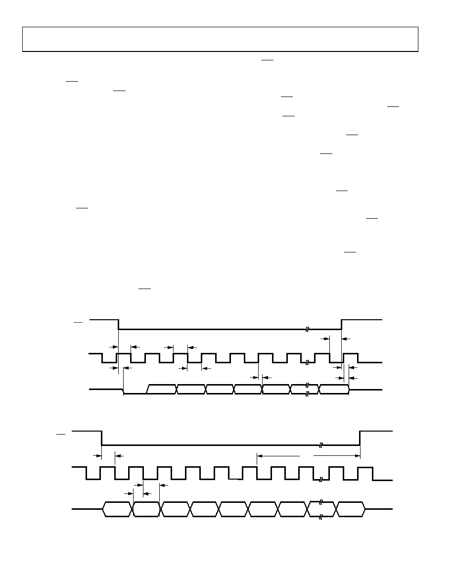
Figure 12 shows the timing diagram for reading from the
AD7890 in the external clocking mode. RFS goes low to access
data from the AD7890. The serial clock input does not have to be
continuous. The serial data can be accessed in a number of bytes.
However, RFS must remain low for the duration of the data
transfer operation. Once again, 16th bits of data are transmitted
with one leading zero, followed by the three address bits in the
control register, followed by the 12-bit conversion result starting
with the MSB. If RFS goes low during the high time of SCLK,
the leading zero is clocked out from the falling edge of RFS (as
per Figure 12). If RFS goes low during the low time of SCLK,
the leading zero is clocked out on the next rising edge of SCLK.
This ensures that, regardless of whether RFS goes low during a
high time or low time of SCLK, the leading zero is valid on the
first falling edge of SCLK after RFS goes low, provided t14 and t17
are adhered to. Serial data is clocked out of the device on the
rising edge of SCLK and is valid on the falling edge of SCLK. At
the end of the read operation, the DATA OUT line is three-stated
by a rising edge on either the SCLK or RFS inputs, whichever
occurs first. If a serial read from the output register is in progress
when conversion is complete, the updating of the output register is
deferred until the serial data read is complete and RFS returns high.
Write Operation
Figure 13 shows a write operation to the control register of the
AD7890. As with self-clocking mode, the TFS input goes low to
indicate to the part that a serial write is about to occur. As before,
the AD7890 control register requires only five bits of data. These
are loaded on the first five clock cycles of the serial clock; data on all
subsequent clock cycles are ignored. However, the part requires six
serial clocks to load data to the control register. Serial data to be
written to the AD7890 must be valid on the falling edge of SCLK.
RFS (I)
SCLK (I)
DATA OUT (O)
NOTES:
1. (I) SIGNIFIES AN INPUT.
2. (O) SIGNIFIES AN OUTPUT.
THREE-STATE
LEADING
ZERO
DB10
DB0
DB11
A2
A1
A0
t14
t13
t15
t16
t17
t19
t19A
t18
01
35
7-
0
12
Figure 12. External Clocking (Slave) Mode Output Register Read
TFS (I)
SCLK (I)
DATA IN (I)
NOTES:
1. (I) SIGNIFIES AN INPUT.
2. (O) SIGNIFIES AN OUTPUT. PULL-UP RESISTOR ON SCLK.
A2
A1
A0
CONV
STBY
DON’T
CARE
DON’T
CARE
DON’T
CARE
t20
t22
t21
t23
01
35
7-
0
13
Figure 13. External Clocking (Slave) Mode Control Register Write
相关PDF资料 |
PDF描述 |
|---|---|
| VI-B1J-IU-F2 | CONVERTER MOD DC/DC 36V 200W |
| AD7890BRZ-2REEL | IC DAS 12BIT 8CH 24-SOIC |
| VE-B1L-IU-F3 | CONVERTER MOD DC/DC 28V 200W |
| VE-B1L-IU-F2 | CONVERTER MOD DC/DC 28V 200W |
| VE-B1L-IU-F1 | CONVERTER MOD DC/DC 28V 200W |
相关代理商/技术参数 |
参数描述 |
|---|---|
| AD7890BRZ-2 | 功能描述:IC DAS 12BIT 8CH 24-SOIC RoHS:是 类别:集成电路 (IC) >> 数据采集 - ADCs/DAC - 专用型 系列:- 产品培训模块:Lead (SnPb) Finish for COTS Obsolescence Mitigation Program 标准包装:50 系列:- 类型:数据采集系统(DAS) 分辨率(位):16 b 采样率(每秒):21.94k 数据接口:MICROWIRE?,QSPI?,串行,SPI? 电压电源:模拟和数字 电源电压:1.8 V ~ 3.6 V 工作温度:-40°C ~ 85°C 安装类型:表面贴装 封装/外壳:40-WFQFN 裸露焊盘 供应商设备封装:40-TQFN-EP(6x6) 包装:托盘 |
| AD7890BRZ-2REEL | 功能描述:IC DAS 12BIT 8CH 24-SOIC RoHS:是 类别:集成电路 (IC) >> 数据采集 - ADCs/DAC - 专用型 系列:- 产品培训模块:Lead (SnPb) Finish for COTS Obsolescence Mitigation Program 标准包装:50 系列:- 类型:数据采集系统(DAS) 分辨率(位):16 b 采样率(每秒):21.94k 数据接口:MICROWIRE?,QSPI?,串行,SPI? 电压电源:模拟和数字 电源电压:1.8 V ~ 3.6 V 工作温度:-40°C ~ 85°C 安装类型:表面贴装 封装/外壳:40-WFQFN 裸露焊盘 供应商设备封装:40-TQFN-EP(6x6) 包装:托盘 |
| AD7890BRZ-4 | 功能描述:IC DAS 12BIT 8CH 24-SOIC RoHS:是 类别:集成电路 (IC) >> 数据采集 - ADCs/DAC - 专用型 系列:- 产品培训模块:Lead (SnPb) Finish for COTS Obsolescence Mitigation Program 标准包装:50 系列:- 类型:数据采集系统(DAS) 分辨率(位):16 b 采样率(每秒):21.94k 数据接口:MICROWIRE?,QSPI?,串行,SPI? 电压电源:模拟和数字 电源电压:1.8 V ~ 3.6 V 工作温度:-40°C ~ 85°C 安装类型:表面贴装 封装/外壳:40-WFQFN 裸露焊盘 供应商设备封装:40-TQFN-EP(6x6) 包装:托盘 |
| AD7890BRZ-4REEL | 功能描述:IC DAS 12BIT 8CH 24-SOIC RoHS:是 类别:集成电路 (IC) >> 数据采集 - ADCs/DAC - 专用型 系列:- 产品培训模块:Lead (SnPb) Finish for COTS Obsolescence Mitigation Program 标准包装:50 系列:- 类型:数据采集系统(DAS) 分辨率(位):16 b 采样率(每秒):21.94k 数据接口:MICROWIRE?,QSPI?,串行,SPI? 电压电源:模拟和数字 电源电压:1.8 V ~ 3.6 V 工作温度:-40°C ~ 85°C 安装类型:表面贴装 封装/外壳:40-WFQFN 裸露焊盘 供应商设备封装:40-TQFN-EP(6x6) 包装:托盘 |
| AD7890SQ-10 | 功能描述:模数转换器 - ADC LC2MOS 8CH 12B Data Acquisition System RoHS:否 制造商:Analog Devices 通道数量: 结构: 转换速率: 分辨率: 输入类型: 信噪比: 接口类型: 工作电源电压: 最大工作温度: 安装风格: 封装 / 箱体: |
发布紧急采购,3分钟左右您将得到回复。