参数资料
| 型号: | AD7890BRZ-10REEL |
| 厂商: | Analog Devices Inc |
| 文件页数: | 4/28页 |
| 文件大小: | 0K |
| 描述: | IC DAS 12BIT 8CH 24-SOIC |
| 产品培训模块: | Power Line Monitoring |
| 标准包装: | 1,000 |
| 类型: | 数据采集系统(DAS) |
| 分辨率(位): | 12 b |
| 采样率(每秒): | 117k |
| 数据接口: | 串行 |
| 电压电源: | 单电源 |
| 电源电压: | 5V |
| 工作温度: | -40°C ~ 85°C |
| 安装类型: | 表面贴装 |
| 封装/外壳: | 24-SOIC(0.295",7.50mm 宽) |
| 供应商设备封装: | 24-SOIC W |
| 包装: | 带卷 (TR) |
第1页第2页第3页当前第4页第5页第6页第7页第8页第9页第10页第11页第12页第13页第14页第15页第16页第17页第18页第19页第20页第21页第22页第23页第24页第25页第26页第27页第28页
AD7890
Rev. C | Page 12 of 28
Table 4. Ideal Input/Output Code Table for the AD7890-10
Analog Input1
Digital Output Code Transition
+FSR/2 1 LSB2 (9.995117 V)
011 . . . 110 to 011 . . . 111
+FSR/2 2 LSBs (9.990234 V)
011 . . . 101 to 011 . . . 110
+FSR/2 3 LSBs (9.985352 V)
011 . . . 100 to 011 . . . 101
AGND + 1 LSB (0.004883 V)
000 . . . 000 to 000 . . . 001
AGND (0.000000 V)
111 . . . 111 to 000 . . . 000
AGND 1 LSB (0.004883 V)
111 . . . 110 to 111 . . . 111
FSR/2 + 3 LSBs (9.985352 V)
100 . . . 010 to 100 . . . 011
FSR/2 + 2 LSBs (9.990234 V)
100 . . . 001 to 100 . . . 010
FSR/2 + 1 LSB (9.995117 V)
100 . . . 000 to 100 . . . 001
1FSR is full-scale range and is 20 V with REF IN = 2.5 V.
21 LSB = FSR/4096 = 4.883 mV with REF IN = 2.5 V.
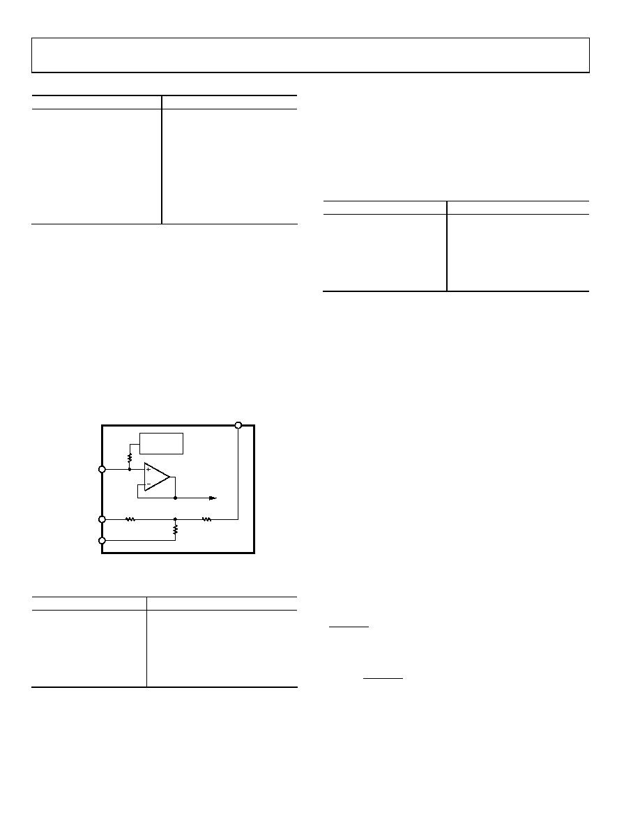
AD7890-4 Analog Input
Figure 5 shows the analog input section for the AD7890-4. The
analog input range for each of the analog inputs is 0 to 4.096 V
into an input resistance of typically 15 kΩ. This input is benign
with no dynamic charging currents with the resistor attenuator
stage followed by the multiplexer and in cases where MUX OUT is
connected to SHA IN this is followed by the high input
impedance stage of the track/hold amplifier. The designed code
transitions occur on successive integer LSB values (such as:
1 LSB, 2 LSBs, 3 LSBs . . . ). Output coding is straight (natural)
binary with 1 LSB = FSR/4096 = 4.096 V/4096 = 1 mV. The
ideal input/output transfer function is shown in Table 5.
2.5V
REFERENCE
6k
2k
2001
9.38k
AD7890-4
REF OUT/
REF IN
AGND
VINX
1EQUIVALENT ON-RESISTANCE OF MULTIPLEXER
MUX OUT
TO ADC
REFERENCE
CIRCUITRY
01
35
7-
0
05
Figure 5. AD7890-4 Analog Input Structure
Table 5. Ideal Input/Output Code Table for the AD7890-4
Analog Input1
Digital Output Code Transition
+FSR 1 LSB2 (4.095 V)
111 . . . 110 to 111 . . . 111
+FSR 2 LSBs (4.094 V)
111 . . . 101 to 111 . . . 110
+FSR 3 LSBs (4.093 V)
111 . . . 100 to 111 . . . 101
AGND + 3 LSBs (0.003 V)
000 . . . 010 to 000 . . . 011
AGND + 2 LSBs (0.002 V)
000 . . . 001 to 000 . . . 010
AGND + 1 LSB (0.001 V)
000 . . . 000 to 000 . . . 001
1FSR is full-scale range and is 4.096 V with REF IN = 2.5 V.
21 LSB = FSR/4096 = 1 mV with REF IN = 2.5 V.
AD7890-2 Analog Input
The analog input section for the AD7890-2 contains no biasing
resistors and the selected analog input connects to the multi-
plexer and, in cases where MUX OUT is connected to SHA IN,
this is followed by the high input impedance stage of the track/
hold amplifier. The analog input range is, therefore, 0 V to 2.5 V
into a high impedance stage with an input current of less than
50 nA. The designed code transitions occur on successive
integer LSB values (such as: l LSB, 2 LSBs, 3 LSBs . . . FS-1
LSBs). Output coding is straight (natural) binary with 1 LSB =
FSR/4096 = 2.5 V/4096 = 0.61 mV. The ideal input/output
transfer function is shown in Table 6.
Table 6. Ideal Input/Output Code Table for the AD7890-2
Analog Input1
Digital Output Code Transition
+FSR 1 LSB2 (2.499390 V)
111 . . . 110 to 111 . . . 111
+FSR 2 LSBs (2.498779 V)
111 . . . 101 to 111 . . . 110
+FSR 3 LSBs (2.498169 V)
111 . . . 100 to 111 . . . 101
AGND + 3 LSBs (0.001831 V)
000 . . . 010 to 010 . . . 011
AGND + 2 LSBs (0.001221 V)
000 . . . 001 to 001 . . . 010
AGND + 1 LSB (0.000610 V)
000 . . . 000 to 000 . . . 001
1FSR is full-scale range and is 2.5 V with REF IN = 2.5 V.
21 LSB = FSR/4096 = 0.61 mV with REF IN = 2.5 V.
TRACK/HOLD AMPLIFIER
The SHA IN input on the AD7890 connects directly to the input
stage of the track/hold amplifier. This is a high impedance input
with input leakage currents of less than 50 nA. Connecting the
MUX OUT pin directly to the SHA IN pin connects the
multiplexer output directly to the track/hold amplifier. The input
voltage range for this input is 0 V to 2.5 V. If external circuitry is
connected between MUX OUT and SHA IN, then the user must
ensure that the input voltage range to the SHA IN input is 0 V to
2.5 V to ensure that the full dynamic range of the converter is
utilized.
The track/hold amplifier on the AD7890 allows the ADC to
accurately convert an input sine wave of full-scale amplitude to
12-bit accuracy. The input bandwidth of the track/hold is
greater than the Nyquist rate of the ADC even when the ADC is
operated at its maximum throughput rate of 117 kHz (for example,
the track/hold can handle input frequencies in excess of 58 kHz).
The track/hold amplifier acquires an input signal to 12-bit
accuracy in less than 2 μs. The operation of the track/hold is
essentially transparent to the user. The track/hold amplifier
goes from its tracking mode to its hold mode at the start of
conversion. The start of conversion is the rising edge of
CONVST (assuming the internal pulse has timed out) for
hardware conversion starts and for software conversion starts is
the point where the internal pulse is timed out. The aperture
time for the track/hold (for example, the delay time between the
external CONVST signal and the track/hold actually going into
hold) is typically 15 ns. For software conversion starts, the time
depends on the internal pulse widths. Therefore, for software
conversion starts, the sampling instant is not very well defined.
For sampling systems which require well defined, equidistant
sampling, it may not be possible to achieve optimum performance
from the part using the software conversion start. At the end of
相关PDF资料 |
PDF描述 |
|---|---|
| VI-B1J-IU-F2 | CONVERTER MOD DC/DC 36V 200W |
| AD7890BRZ-2REEL | IC DAS 12BIT 8CH 24-SOIC |
| VE-B1L-IU-F3 | CONVERTER MOD DC/DC 28V 200W |
| VE-B1L-IU-F2 | CONVERTER MOD DC/DC 28V 200W |
| VE-B1L-IU-F1 | CONVERTER MOD DC/DC 28V 200W |
相关代理商/技术参数 |
参数描述 |
|---|---|
| AD7890BRZ-2 | 功能描述:IC DAS 12BIT 8CH 24-SOIC RoHS:是 类别:集成电路 (IC) >> 数据采集 - ADCs/DAC - 专用型 系列:- 产品培训模块:Lead (SnPb) Finish for COTS Obsolescence Mitigation Program 标准包装:50 系列:- 类型:数据采集系统(DAS) 分辨率(位):16 b 采样率(每秒):21.94k 数据接口:MICROWIRE?,QSPI?,串行,SPI? 电压电源:模拟和数字 电源电压:1.8 V ~ 3.6 V 工作温度:-40°C ~ 85°C 安装类型:表面贴装 封装/外壳:40-WFQFN 裸露焊盘 供应商设备封装:40-TQFN-EP(6x6) 包装:托盘 |
| AD7890BRZ-2REEL | 功能描述:IC DAS 12BIT 8CH 24-SOIC RoHS:是 类别:集成电路 (IC) >> 数据采集 - ADCs/DAC - 专用型 系列:- 产品培训模块:Lead (SnPb) Finish for COTS Obsolescence Mitigation Program 标准包装:50 系列:- 类型:数据采集系统(DAS) 分辨率(位):16 b 采样率(每秒):21.94k 数据接口:MICROWIRE?,QSPI?,串行,SPI? 电压电源:模拟和数字 电源电压:1.8 V ~ 3.6 V 工作温度:-40°C ~ 85°C 安装类型:表面贴装 封装/外壳:40-WFQFN 裸露焊盘 供应商设备封装:40-TQFN-EP(6x6) 包装:托盘 |
| AD7890BRZ-4 | 功能描述:IC DAS 12BIT 8CH 24-SOIC RoHS:是 类别:集成电路 (IC) >> 数据采集 - ADCs/DAC - 专用型 系列:- 产品培训模块:Lead (SnPb) Finish for COTS Obsolescence Mitigation Program 标准包装:50 系列:- 类型:数据采集系统(DAS) 分辨率(位):16 b 采样率(每秒):21.94k 数据接口:MICROWIRE?,QSPI?,串行,SPI? 电压电源:模拟和数字 电源电压:1.8 V ~ 3.6 V 工作温度:-40°C ~ 85°C 安装类型:表面贴装 封装/外壳:40-WFQFN 裸露焊盘 供应商设备封装:40-TQFN-EP(6x6) 包装:托盘 |
| AD7890BRZ-4REEL | 功能描述:IC DAS 12BIT 8CH 24-SOIC RoHS:是 类别:集成电路 (IC) >> 数据采集 - ADCs/DAC - 专用型 系列:- 产品培训模块:Lead (SnPb) Finish for COTS Obsolescence Mitigation Program 标准包装:50 系列:- 类型:数据采集系统(DAS) 分辨率(位):16 b 采样率(每秒):21.94k 数据接口:MICROWIRE?,QSPI?,串行,SPI? 电压电源:模拟和数字 电源电压:1.8 V ~ 3.6 V 工作温度:-40°C ~ 85°C 安装类型:表面贴装 封装/外壳:40-WFQFN 裸露焊盘 供应商设备封装:40-TQFN-EP(6x6) 包装:托盘 |
| AD7890SQ-10 | 功能描述:模数转换器 - ADC LC2MOS 8CH 12B Data Acquisition System RoHS:否 制造商:Analog Devices 通道数量: 结构: 转换速率: 分辨率: 输入类型: 信噪比: 接口类型: 工作电源电压: 最大工作温度: 安装风格: 封装 / 箱体: |
发布紧急采购,3分钟左右您将得到回复。