参数资料
| 型号: | AD7890BRZ-10REEL |
| 厂商: | Analog Devices Inc |
| 文件页数: | 3/28页 |
| 文件大小: | 0K |
| 描述: | IC DAS 12BIT 8CH 24-SOIC |
| 产品培训模块: | Power Line Monitoring |
| 标准包装: | 1,000 |
| 类型: | 数据采集系统(DAS) |
| 分辨率(位): | 12 b |
| 采样率(每秒): | 117k |
| 数据接口: | 串行 |
| 电压电源: | 单电源 |
| 电源电压: | 5V |
| 工作温度: | -40°C ~ 85°C |
| 安装类型: | 表面贴装 |
| 封装/外壳: | 24-SOIC(0.295",7.50mm 宽) |
| 供应商设备封装: | 24-SOIC W |
| 包装: | 带卷 (TR) |
第1页第2页当前第3页第4页第5页第6页第7页第8页第9页第10页第11页第12页第13页第14页第15页第16页第17页第18页第19页第20页第21页第22页第23页第24页第25页第26页第27页第28页
AD7890
Rev. C | Page 11 of 28
THEORY OF OPERATION
CONVERTER DETAILS
The AD7890 is an 8-channel, 12-bit, single supply, serial data
acquisition system. It provides the user with signal scaling,
multiplexer, track/hold, reference, ADC, and versatile serial
logic functions on a single chip. The signal scaling allows the
part to handle ±10 V input signals (AD7890-10) and 0 V to
4.096 V input signals (AD7890-4) while operating from a single
5 V supply. The AD7890-2 contains no signal scaling and
accepts an analog input range of 0 V to 2.5 V. The part operates
from a 2.5 V reference, which can be provided from the part’s
own internal reference or from an external reference source.
Unlike other single chip data acquisition solutions, the AD7890
provides the user with separate access to the multiplexer and
the ADC. This means that the flexibility of separate multiplexer
and ADC solutions is not sacrificed with the one-chip solution.
With access to the multiplexer output, the user can implement
external signal conditioning between the multiplexer and the
track/hold. It means that one antialiasing filter can be used on
the output of the multiplexer to provide the antialiasing
function for all eight channels.
Conversion is initiated on the AD7890 either by pulsing the
CONVST input or by writing a Logic 1 to the CONV bit of the
control register. When using the hardware CONVST input, on
the rising edge of the CONVST signal, the on-chip track/hold
goes from track to hold mode and the conversion sequence is
started, provided the internal pulse has timed out. This internal
pulse (which appears at the CEXT pin) is initiated whenever the
multiplexer address is loaded to the AD7890 control register.
This pulse goes from high to low when a serial write to the part
is initiated. It starts to discharge on the sixth falling clock edge
of SCLK in a serial write operation to the part. The track/hold
cannot go into hold and conversion cannot be initiated until the
CEXT pin has crossed its trigger point of 2.5 V. The discharge
time of the voltage on CEXT depends upon the value of capacitor
connected to the CEXT pin (see the CEXT Functioning section).
The fact that the pulse is initiated every time a write to the
control register takes place means that the software conversion
start and track/hold signal is always delayed by the internal pulse.
The conversion clock for the part is generated from the clock
signal applied to the CLK IN pin of the part. Conversion time
for the AD7890 is 5.9 μs from the rising edge of the hardware
CONVST signal and the track/hold acquisition time is 2 μs. To
obtain optimum performance from the part, the data read
operation or control register write operation should not occur
during the conversion or during 500 ns prior to the next
conversion.
This allows the part to operate at throughput rates up to
117 kHz in the external clocking mode and achieve data sheet
specifications. The part can operate at slightly higher
throughput rates (up to 127 kHz), again in external clocking
mode with degraded performance (see the Timing and Control
section). The throughput rate for self-clocking mode is limited
by the serial clock rate to 78 kHz.
All unused inputs should be connected to a voltage within the
nominal analog input range to avoid noise pickup. On the
AD7890-10, if any one of the input channels which are not
being converted goes more negative than 12 V, it can interfere
with the conversion on the selected channel.
CIRCUIT DESCRIPTION
The AD7890 is offered as three part types: the AD7890-10
handles a ±10 V input voltage range, the AD7890-4 handles a
0 V to 4.096 V input range, while the AD7890-2 handles a 0 V
to 2.5 V input voltage range.
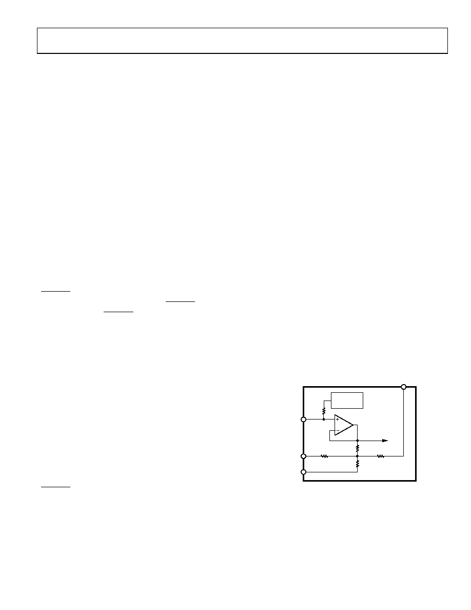
AD7890-10 Analog Input
Figure 4 shows the analog input section for the AD7890-10. The
analog input range for each of the analog inputs is ±10 V into
an input resistance of typically 33 kΩ. This input is benign with
no dynamic charging currents with the resistor attenuator stage
followed by the multiplexer and, in cases where MUX OUT is
connected to SHA IN, this is followed by the high input
impedance stage of the track/hold amplifier. The designed code
transitions occur on successive integer LSB values (such as:
1 LSB, 2 LSBs, 3 LSBs...). Output coding is twos complement
binary with 1 LSB FSR/4096 = 20 V/4096 = 4.88 mV. The
ideal input/output transfer function is shown in Table 4.
2.5V
REFERENCE
30k
2k
7.5k
2001
10k
AD7890-10
REF OUT/
REF IN
AGND
VINX
1EQUIVALENT ON-RESISTANCE OF MULTIPLEXER
MUX OUT
TO ADC
REFERENCE
CIRCUITRY
01
35
7-
0
4
Figure 4. AD7890-10 Analog Input Structure
相关PDF资料 |
PDF描述 |
|---|---|
| VI-B1J-IU-F2 | CONVERTER MOD DC/DC 36V 200W |
| AD7890BRZ-2REEL | IC DAS 12BIT 8CH 24-SOIC |
| VE-B1L-IU-F3 | CONVERTER MOD DC/DC 28V 200W |
| VE-B1L-IU-F2 | CONVERTER MOD DC/DC 28V 200W |
| VE-B1L-IU-F1 | CONVERTER MOD DC/DC 28V 200W |
相关代理商/技术参数 |
参数描述 |
|---|---|
| AD7890BRZ-2 | 功能描述:IC DAS 12BIT 8CH 24-SOIC RoHS:是 类别:集成电路 (IC) >> 数据采集 - ADCs/DAC - 专用型 系列:- 产品培训模块:Lead (SnPb) Finish for COTS Obsolescence Mitigation Program 标准包装:50 系列:- 类型:数据采集系统(DAS) 分辨率(位):16 b 采样率(每秒):21.94k 数据接口:MICROWIRE?,QSPI?,串行,SPI? 电压电源:模拟和数字 电源电压:1.8 V ~ 3.6 V 工作温度:-40°C ~ 85°C 安装类型:表面贴装 封装/外壳:40-WFQFN 裸露焊盘 供应商设备封装:40-TQFN-EP(6x6) 包装:托盘 |
| AD7890BRZ-2REEL | 功能描述:IC DAS 12BIT 8CH 24-SOIC RoHS:是 类别:集成电路 (IC) >> 数据采集 - ADCs/DAC - 专用型 系列:- 产品培训模块:Lead (SnPb) Finish for COTS Obsolescence Mitigation Program 标准包装:50 系列:- 类型:数据采集系统(DAS) 分辨率(位):16 b 采样率(每秒):21.94k 数据接口:MICROWIRE?,QSPI?,串行,SPI? 电压电源:模拟和数字 电源电压:1.8 V ~ 3.6 V 工作温度:-40°C ~ 85°C 安装类型:表面贴装 封装/外壳:40-WFQFN 裸露焊盘 供应商设备封装:40-TQFN-EP(6x6) 包装:托盘 |
| AD7890BRZ-4 | 功能描述:IC DAS 12BIT 8CH 24-SOIC RoHS:是 类别:集成电路 (IC) >> 数据采集 - ADCs/DAC - 专用型 系列:- 产品培训模块:Lead (SnPb) Finish for COTS Obsolescence Mitigation Program 标准包装:50 系列:- 类型:数据采集系统(DAS) 分辨率(位):16 b 采样率(每秒):21.94k 数据接口:MICROWIRE?,QSPI?,串行,SPI? 电压电源:模拟和数字 电源电压:1.8 V ~ 3.6 V 工作温度:-40°C ~ 85°C 安装类型:表面贴装 封装/外壳:40-WFQFN 裸露焊盘 供应商设备封装:40-TQFN-EP(6x6) 包装:托盘 |
| AD7890BRZ-4REEL | 功能描述:IC DAS 12BIT 8CH 24-SOIC RoHS:是 类别:集成电路 (IC) >> 数据采集 - ADCs/DAC - 专用型 系列:- 产品培训模块:Lead (SnPb) Finish for COTS Obsolescence Mitigation Program 标准包装:50 系列:- 类型:数据采集系统(DAS) 分辨率(位):16 b 采样率(每秒):21.94k 数据接口:MICROWIRE?,QSPI?,串行,SPI? 电压电源:模拟和数字 电源电压:1.8 V ~ 3.6 V 工作温度:-40°C ~ 85°C 安装类型:表面贴装 封装/外壳:40-WFQFN 裸露焊盘 供应商设备封装:40-TQFN-EP(6x6) 包装:托盘 |
| AD7890SQ-10 | 功能描述:模数转换器 - ADC LC2MOS 8CH 12B Data Acquisition System RoHS:否 制造商:Analog Devices 通道数量: 结构: 转换速率: 分辨率: 输入类型: 信噪比: 接口类型: 工作电源电压: 最大工作温度: 安装风格: 封装 / 箱体: |
发布紧急采购,3分钟左右您将得到回复。