参数资料
| 型号: | AD7890BRZ-10REEL |
| 厂商: | Analog Devices Inc |
| 文件页数: | 16/28页 |
| 文件大小: | 0K |
| 描述: | IC DAS 12BIT 8CH 24-SOIC |
| 产品培训模块: | Power Line Monitoring |
| 标准包装: | 1,000 |
| 类型: | 数据采集系统(DAS) |
| 分辨率(位): | 12 b |
| 采样率(每秒): | 117k |
| 数据接口: | 串行 |
| 电压电源: | 单电源 |
| 电源电压: | 5V |
| 工作温度: | -40°C ~ 85°C |
| 安装类型: | 表面贴装 |
| 封装/外壳: | 24-SOIC(0.295",7.50mm 宽) |
| 供应商设备封装: | 24-SOIC W |
| 包装: | 带卷 (TR) |
第1页第2页第3页第4页第5页第6页第7页第8页第9页第10页第11页第12页第13页第14页第15页当前第16页第17页第18页第19页第20页第21页第22页第23页第24页第25页第26页第27页第28页
AD7890
Rev. C | Page 23 of 28
PERFORMANCE
LINEARITY
The linearity of the AD7890 is primarily determined by the on-
chip 12-bit D/A converter. This is a segmented DAC that is laser
trimmed for 12-bit integral linearity and differential linearity.
Typical relative numbers for the part are ±1/4 LSB while the
typical DNL errors are ±1/2 LSB.
NOISE
In an ADC, noise exhibits itself as code uncertainty in dc
applications and as the noise floor (in an FFT, for example) in ac
applications. In a sampling ADC like the AD7890, all information
about the analog input appears in the baseband from dc to 1/2 the
sampling frequency. The input bandwidth of the track/hold exceeds
the Nyquist bandwidth and, therefore, an antialiasing filter should
be used to remove unwanted signals above fS/2 in the input signal
in applications where such signals exist.
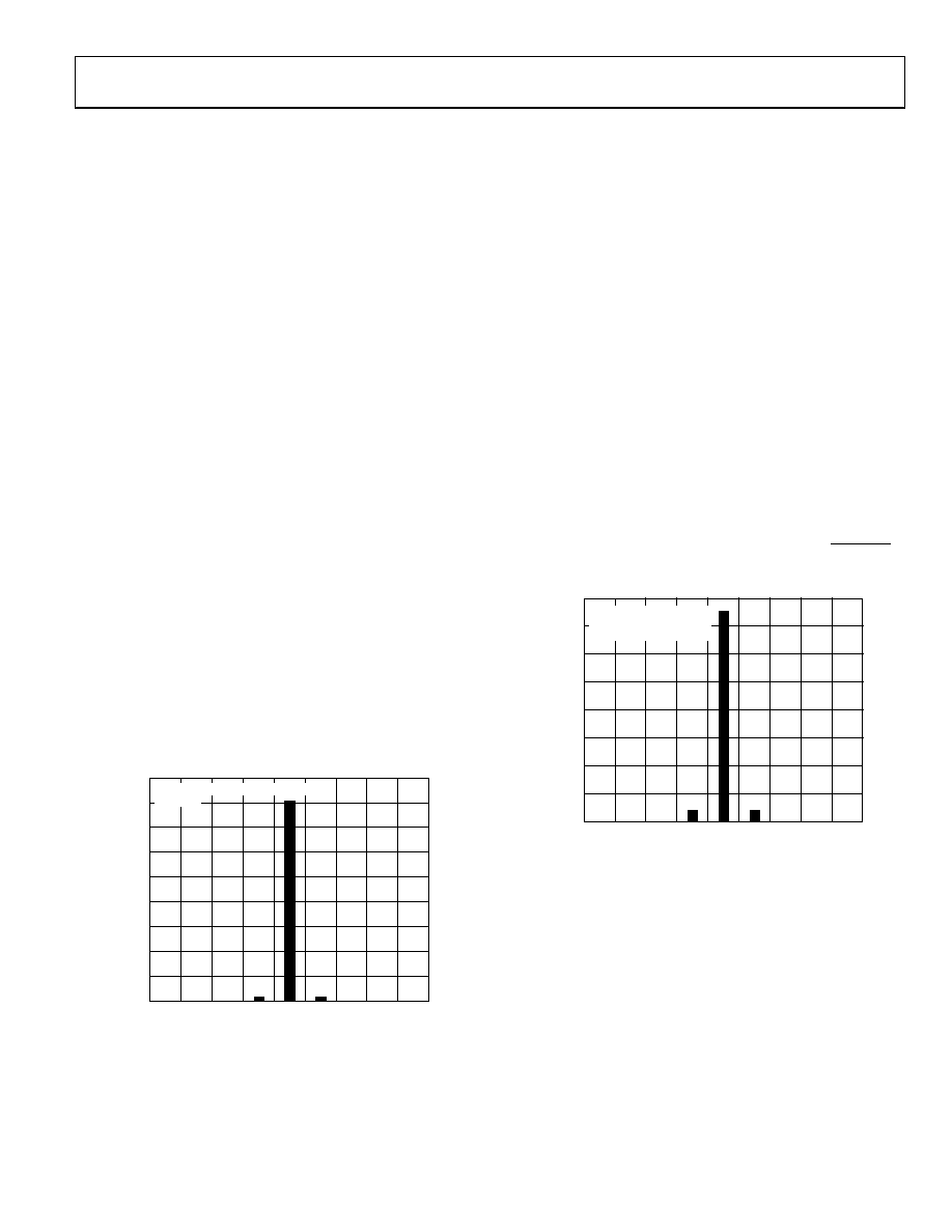
Figure 19 shows a histogram plot for 8192 conversions of a dc
input using the AD7890. The analog input was set at the center
of a code transition. The timing and control sequence used was
as per Figure 7 where the optimum performance of the ADC is
achieved. The same performance can be achieved in self-
clocking mode where the part transmits its data after
conversion is complete. Almost all of the codes appear in the
one output bin indicating very good noise performance from
the ADC. The rms noise performance for the AD7890-2 for the
plot in Figure 19 was 81 μV. Since the analog input range, and
hence LSB size, on the AD7893-4 is 1.638 times what it is for
the AD7893-2, the same output code distribution results in an
output rms noise of 143 μV for the AD7893-4. For the AD7890-10,
with an LSB size eight times that of the AD7890-2, the code
distribution represents an output rms noise of 648 μV.
9000
8000
7000
6000
5000
4000
3000
2000
1000
0
SAMPLING FREQUENCY = 102.4kHz
TA = 25°C
(X–4) (X–3) (X–2) (X–1)
X
(X+1) (X+2) (X+3) (X+4)
O
CC
URRE
N
CE
S
O
F
CO
DE
CODE
0
135
7-
0
19
Figure 19. Histogram of 8192 Conversions of a DC Input
In the external clocking mode, it is possible to write data to the
control register or read data from the output register while a
conversion is in progress. The same data is presented in
Figure 20 as in Figure 19, except that in Figure 20, the output
data read for the device occurs during conversion. These results
are achieved with a serial clock rate of 2.5 MHz. If a higher
serial clock rate is used, the code transition noise degrades from
that shown in the plot in Figure 20. This has the effect of
injecting noise onto the die while bit decisions are being made,
increasing the noise generated by the AD7890. The histogram
plot for 8192 conversions of the same dc input now shows a
larger spread of codes with the rms noise for the AD7890-2
increasing to 170 μV. This effect varies depending on where the
serial clock edges appear with respect to the bit trials of the
conversion process.
It is possible to achieve the same level of performance when
reading during conversion as when reading after conversion,
depending on the relationship of the serial clock edges to the bit
trial points (for example, the relationship of the serial clock
edges to the CLK IN edges). The bit decision points on the
AD7890 are on the falling edges of the master clock (CLK IN)
during the conversion process. Clocking out new data bits at
these points (for example, the rising edge of SCLK) is the most
critical from a noise standpoint. The most critical bit decisions
are the MSBs, so to achieve the level of performance outlined in
Figure 20, reading within 1 μs after the rising edge of CONVST
should be avoided.
8000
7000
6000
5000
4000
3000
2000
1000
0
(X–4) (X–3) (X–2) (X–1)
X
(X+1) (X+2) (X+3) (X+4)
O
CCURR
E
NCE
S
O
F
CO
DE
CODE
SAMPLING
FREQUENCY = 102.4kHz
TA = 25°C
01
35
7-
02
0
Figure 20. Histogram of 8192 Conversions with Read During Conversion
Writing data to the control register also has the effect of
introducing digital activity onto the part while conversion is in
progress. However, since there are no output drivers active
during a write operation, the amount of current flowing on the
die is less than for a read operation. Therefore, the amount of
noise injected into the die is less than for a read operation.
Figure 21 shows the effect of a write operation during
conversion. The histogram plot for 8192 conversions of the
same dc input now shows a larger spread of codes than for ideal
conditions but smaller than for a read operation. The resulting
rms noise for the AD7890-2 is 110 μV. In this case, the serial
clock frequency is 10 MHz.
相关PDF资料 |
PDF描述 |
|---|---|
| VI-B1J-IU-F2 | CONVERTER MOD DC/DC 36V 200W |
| AD7890BRZ-2REEL | IC DAS 12BIT 8CH 24-SOIC |
| VE-B1L-IU-F3 | CONVERTER MOD DC/DC 28V 200W |
| VE-B1L-IU-F2 | CONVERTER MOD DC/DC 28V 200W |
| VE-B1L-IU-F1 | CONVERTER MOD DC/DC 28V 200W |
相关代理商/技术参数 |
参数描述 |
|---|---|
| AD7890BRZ-2 | 功能描述:IC DAS 12BIT 8CH 24-SOIC RoHS:是 类别:集成电路 (IC) >> 数据采集 - ADCs/DAC - 专用型 系列:- 产品培训模块:Lead (SnPb) Finish for COTS Obsolescence Mitigation Program 标准包装:50 系列:- 类型:数据采集系统(DAS) 分辨率(位):16 b 采样率(每秒):21.94k 数据接口:MICROWIRE?,QSPI?,串行,SPI? 电压电源:模拟和数字 电源电压:1.8 V ~ 3.6 V 工作温度:-40°C ~ 85°C 安装类型:表面贴装 封装/外壳:40-WFQFN 裸露焊盘 供应商设备封装:40-TQFN-EP(6x6) 包装:托盘 |
| AD7890BRZ-2REEL | 功能描述:IC DAS 12BIT 8CH 24-SOIC RoHS:是 类别:集成电路 (IC) >> 数据采集 - ADCs/DAC - 专用型 系列:- 产品培训模块:Lead (SnPb) Finish for COTS Obsolescence Mitigation Program 标准包装:50 系列:- 类型:数据采集系统(DAS) 分辨率(位):16 b 采样率(每秒):21.94k 数据接口:MICROWIRE?,QSPI?,串行,SPI? 电压电源:模拟和数字 电源电压:1.8 V ~ 3.6 V 工作温度:-40°C ~ 85°C 安装类型:表面贴装 封装/外壳:40-WFQFN 裸露焊盘 供应商设备封装:40-TQFN-EP(6x6) 包装:托盘 |
| AD7890BRZ-4 | 功能描述:IC DAS 12BIT 8CH 24-SOIC RoHS:是 类别:集成电路 (IC) >> 数据采集 - ADCs/DAC - 专用型 系列:- 产品培训模块:Lead (SnPb) Finish for COTS Obsolescence Mitigation Program 标准包装:50 系列:- 类型:数据采集系统(DAS) 分辨率(位):16 b 采样率(每秒):21.94k 数据接口:MICROWIRE?,QSPI?,串行,SPI? 电压电源:模拟和数字 电源电压:1.8 V ~ 3.6 V 工作温度:-40°C ~ 85°C 安装类型:表面贴装 封装/外壳:40-WFQFN 裸露焊盘 供应商设备封装:40-TQFN-EP(6x6) 包装:托盘 |
| AD7890BRZ-4REEL | 功能描述:IC DAS 12BIT 8CH 24-SOIC RoHS:是 类别:集成电路 (IC) >> 数据采集 - ADCs/DAC - 专用型 系列:- 产品培训模块:Lead (SnPb) Finish for COTS Obsolescence Mitigation Program 标准包装:50 系列:- 类型:数据采集系统(DAS) 分辨率(位):16 b 采样率(每秒):21.94k 数据接口:MICROWIRE?,QSPI?,串行,SPI? 电压电源:模拟和数字 电源电压:1.8 V ~ 3.6 V 工作温度:-40°C ~ 85°C 安装类型:表面贴装 封装/外壳:40-WFQFN 裸露焊盘 供应商设备封装:40-TQFN-EP(6x6) 包装:托盘 |
| AD7890SQ-10 | 功能描述:模数转换器 - ADC LC2MOS 8CH 12B Data Acquisition System RoHS:否 制造商:Analog Devices 通道数量: 结构: 转换速率: 分辨率: 输入类型: 信噪比: 接口类型: 工作电源电压: 最大工作温度: 安装风格: 封装 / 箱体: |
发布紧急采购,3分钟左右您将得到回复。