参数资料
| 型号: | AD7890BRZ-10REEL |
| 厂商: | Analog Devices Inc |
| 文件页数: | 26/28页 |
| 文件大小: | 0K |
| 描述: | IC DAS 12BIT 8CH 24-SOIC |
| 产品培训模块: | Power Line Monitoring |
| 标准包装: | 1,000 |
| 类型: | 数据采集系统(DAS) |
| 分辨率(位): | 12 b |
| 采样率(每秒): | 117k |
| 数据接口: | 串行 |
| 电压电源: | 单电源 |
| 电源电压: | 5V |
| 工作温度: | -40°C ~ 85°C |
| 安装类型: | 表面贴装 |
| 封装/外壳: | 24-SOIC(0.295",7.50mm 宽) |
| 供应商设备封装: | 24-SOIC W |
| 包装: | 带卷 (TR) |
第1页第2页第3页第4页第5页第6页第7页第8页第9页第10页第11页第12页第13页第14页第15页第16页第17页第18页第19页第20页第21页第22页第23页第24页第25页当前第26页第27页第28页
AD7890
Rev. C | Page 7 of 28
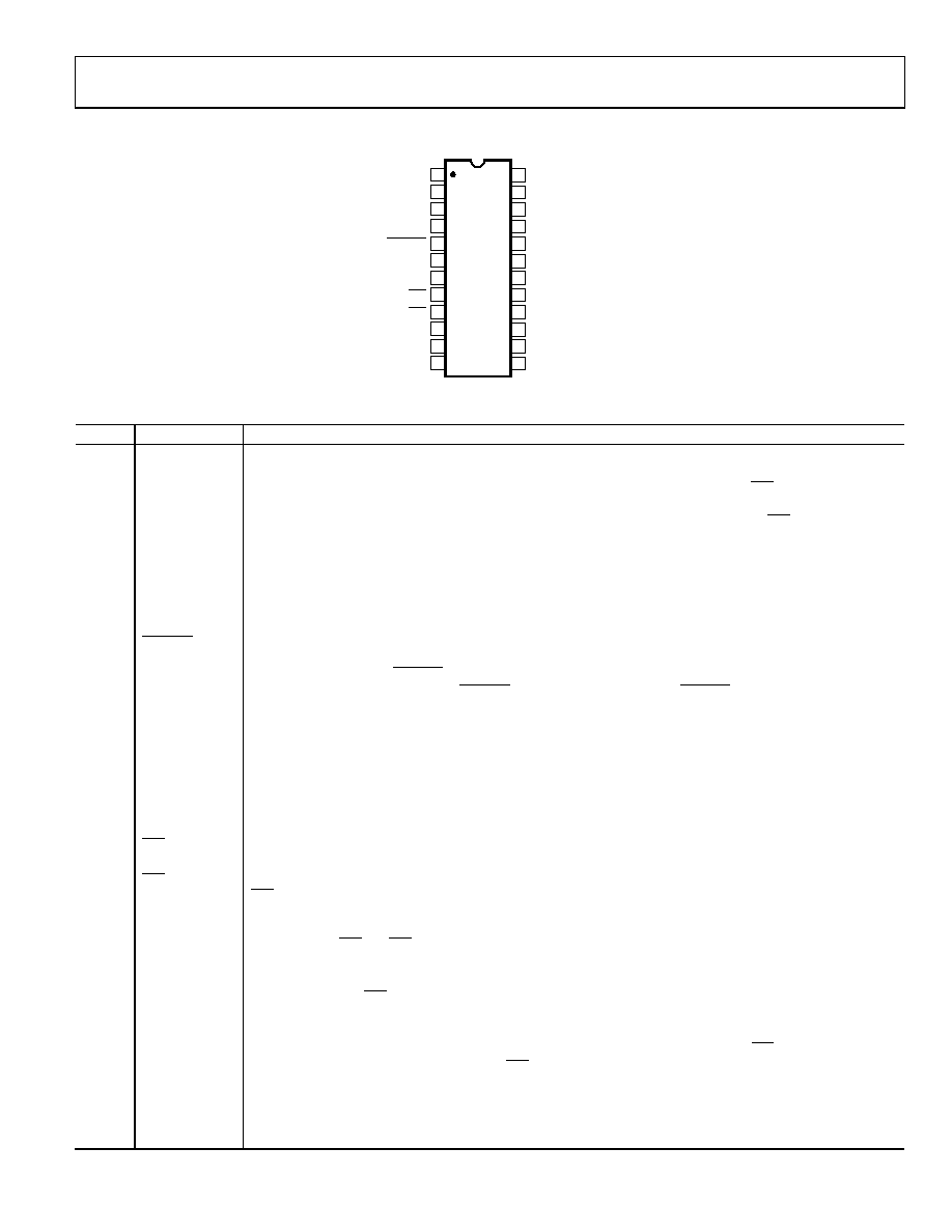
PIN CONFIGURATION AND FUNCTION DESCRIPTIONS
24
23
22
21
20
19
18
17
16
15
14
13
1
2
3
4
5
6
7
8
9
10
11
12
REF OUT/REF IN
CONVST
TFS
RFS
DATA OUT
DATA IN
VDD
VIN8
VIN7
VIN6
VIN5
VIN4
VIN3
VIN2
VIN1
AD7890
TOP VIEW
(Not to Scale)
AGND
SHA IN
MUX OUT
DGND
CLK IN
SCLK
CEXT
SMODE
01
357
-00
3
Figure 3. Pin Configuration
Table 2. Pin Function Descriptions
Pin No.
Mnemonic
Description
1
AGND
Analog Ground. Ground reference for track/hold, comparator, and DAC.
2
SMODE
Control Input. Determines whether the part operates in its external clocking (slave) or self-clocking (master)
serial mode. With SMODE at a logic low, the part is in its self-clocking serial mode with RFS and SCLK as
outputs. This self-clocking mode is useful for connection to shift registers or to serial ports of DSP processors.
With SMODE at a logic high, the part is in its external clocking serial mode with SCLK and RFS as inputs. This
external clocking mode is useful for connection to the serial port of microcontrollers, such as the 8xC51 and
the 68HCxx, and for connection to the serial ports of DSP processors.
3
DGND
Digital Ground. Ground reference for digital circuitry.
4
CEXT
External Capacitor. An external capacitor is connected to this pin to determine the length of the internal pulse
(see the Control Register section). Larger capacitances on this pin extend the pulse to allow for settling time
delays through an external antialiasing filter or signal conditioning circuitry.
5
CONVST
Convert Start. Edge-triggered logic input. A low-to-high transition on this input puts the track/hold into hold
and initiates conversion if the internal pulse has timed out (see the Control Register section). If the internal
pulse is active when the CONVST goes high, the track/hold does not proceed to hold until the pulse times out.
If the internal pulse times out when CONVST goes high, the rising edge of CONVST drives the track/hold into
hold and initiates conversion.
6
CLK IN
Clock Input. An external TTL-compatible clock is applied to this input pin to provide the clock source for the
conversion sequence. In the self-clocking serial mode, the SCLK output is derived from this CLK IN pin.
7
SCLK
Serial Clock Input. In the external clocking (slave) mode (see the Serial Interface section), this is an externally
applied serial clock used to load serial data to the control register and to access data from the output register.
In the self-clocking (master) mode, the internal serial clock, which is derived from the clock input (CLK IN),
appears on this pin. Once again, it is used to load serial data to the control register and to access data from the
output register.
8
TFS
Transmit Frame Synchronization Pulse. Active low logic input with serial data expected after the falling edge of
this signal.
9
RFS
Receive Frame Synchronization Pulse. In the external clocking mode, this pin is an active low logic input with
RFS provided externally as a strobe or framing pulse to access serial data from the output register. In the self-
clocking mode, it is an active low output, which is internally generated and provides a strobe or framing pulse
for serial data from the output register. For applications which require that data be transmitted and received at
the same time, RFS and TFS should be connected together.
10
DATA OUT
Serial Data Output. Sixteen bits of serial data are provided with one leading zero, preceding the three address
bits of the control register and the 12 bits of conversion data. Serial data is valid on the falling edge of SCLK for
sixteen edges after RFS goes low. Output coding from the ADC is twos complement for the AD7890-10 and
straight binary for the AD7890-4 and AD7890-2.
11
DATA IN
Serial Data Input. Serial data to be loaded to the control register is provided at this input. The first five bits of
serial data are loaded to the control register on the first five falling edges of SCLK after TFS goes low. Serial data
on subsequent SCLK edges is ignored while TFS remains low.
12
VDD
Positive Supply Voltage, 5 V ± 5%.
13
MUX OUT
Multiplexer Output. The output of the multiplexer appears at this pin. The output voltage range from this
output is 0 V to 2.5 V for the nominal analog input range to the selected channel. The output impedance of this
output is nominally 3.5 kΩ. If no external antialiasing filter is required, MUX OUT should be connected to SHA IN.
相关PDF资料 |
PDF描述 |
|---|---|
| VI-B1J-IU-F2 | CONVERTER MOD DC/DC 36V 200W |
| AD7890BRZ-2REEL | IC DAS 12BIT 8CH 24-SOIC |
| VE-B1L-IU-F3 | CONVERTER MOD DC/DC 28V 200W |
| VE-B1L-IU-F2 | CONVERTER MOD DC/DC 28V 200W |
| VE-B1L-IU-F1 | CONVERTER MOD DC/DC 28V 200W |
相关代理商/技术参数 |
参数描述 |
|---|---|
| AD7890BRZ-2 | 功能描述:IC DAS 12BIT 8CH 24-SOIC RoHS:是 类别:集成电路 (IC) >> 数据采集 - ADCs/DAC - 专用型 系列:- 产品培训模块:Lead (SnPb) Finish for COTS Obsolescence Mitigation Program 标准包装:50 系列:- 类型:数据采集系统(DAS) 分辨率(位):16 b 采样率(每秒):21.94k 数据接口:MICROWIRE?,QSPI?,串行,SPI? 电压电源:模拟和数字 电源电压:1.8 V ~ 3.6 V 工作温度:-40°C ~ 85°C 安装类型:表面贴装 封装/外壳:40-WFQFN 裸露焊盘 供应商设备封装:40-TQFN-EP(6x6) 包装:托盘 |
| AD7890BRZ-2REEL | 功能描述:IC DAS 12BIT 8CH 24-SOIC RoHS:是 类别:集成电路 (IC) >> 数据采集 - ADCs/DAC - 专用型 系列:- 产品培训模块:Lead (SnPb) Finish for COTS Obsolescence Mitigation Program 标准包装:50 系列:- 类型:数据采集系统(DAS) 分辨率(位):16 b 采样率(每秒):21.94k 数据接口:MICROWIRE?,QSPI?,串行,SPI? 电压电源:模拟和数字 电源电压:1.8 V ~ 3.6 V 工作温度:-40°C ~ 85°C 安装类型:表面贴装 封装/外壳:40-WFQFN 裸露焊盘 供应商设备封装:40-TQFN-EP(6x6) 包装:托盘 |
| AD7890BRZ-4 | 功能描述:IC DAS 12BIT 8CH 24-SOIC RoHS:是 类别:集成电路 (IC) >> 数据采集 - ADCs/DAC - 专用型 系列:- 产品培训模块:Lead (SnPb) Finish for COTS Obsolescence Mitigation Program 标准包装:50 系列:- 类型:数据采集系统(DAS) 分辨率(位):16 b 采样率(每秒):21.94k 数据接口:MICROWIRE?,QSPI?,串行,SPI? 电压电源:模拟和数字 电源电压:1.8 V ~ 3.6 V 工作温度:-40°C ~ 85°C 安装类型:表面贴装 封装/外壳:40-WFQFN 裸露焊盘 供应商设备封装:40-TQFN-EP(6x6) 包装:托盘 |
| AD7890BRZ-4REEL | 功能描述:IC DAS 12BIT 8CH 24-SOIC RoHS:是 类别:集成电路 (IC) >> 数据采集 - ADCs/DAC - 专用型 系列:- 产品培训模块:Lead (SnPb) Finish for COTS Obsolescence Mitigation Program 标准包装:50 系列:- 类型:数据采集系统(DAS) 分辨率(位):16 b 采样率(每秒):21.94k 数据接口:MICROWIRE?,QSPI?,串行,SPI? 电压电源:模拟和数字 电源电压:1.8 V ~ 3.6 V 工作温度:-40°C ~ 85°C 安装类型:表面贴装 封装/外壳:40-WFQFN 裸露焊盘 供应商设备封装:40-TQFN-EP(6x6) 包装:托盘 |
| AD7890SQ-10 | 功能描述:模数转换器 - ADC LC2MOS 8CH 12B Data Acquisition System RoHS:否 制造商:Analog Devices 通道数量: 结构: 转换速率: 分辨率: 输入类型: 信噪比: 接口类型: 工作电源电压: 最大工作温度: 安装风格: 封装 / 箱体: |
发布紧急采购,3分钟左右您将得到回复。