- 您现在的位置:买卖IC网 > PDF目录10252 > AD7934BRUZ-REEL7 (Analog Devices Inc)IC ADC 12BIT 4CH 1.5MSPS 28TSSOP PDF资料下载
参数资料
| 型号: | AD7934BRUZ-REEL7 |
| 厂商: | Analog Devices Inc |
| 文件页数: | 14/32页 |
| 文件大小: | 0K |
| 描述: | IC ADC 12BIT 4CH 1.5MSPS 28TSSOP |
| 标准包装: | 1,000 |
| 位数: | 12 |
| 采样率(每秒): | 1.5M |
| 数据接口: | 并联 |
| 转换器数目: | 1 |
| 功率耗散(最大): | 13.5mW |
| 电压电源: | 单电源 |
| 工作温度: | -40°C ~ 85°C |
| 安装类型: | 表面贴装 |
| 封装/外壳: | 28-TSSOP(0.173",4.40mm 宽) |
| 供应商设备封装: | 28-TSSOP |
| 包装: | 带卷 (TR) |
| 输入数目和类型: | 4 个单端,单极;2 个差分,单极;2 个伪差分,单极 |
第1页第2页第3页第4页第5页第6页第7页第8页第9页第10页第11页第12页第13页当前第14页第15页第16页第17页第18页第19页第20页第21页第22页第23页第24页第25页第26页第27页第28页第29页第30页第31页第32页
AD7933/AD7934
Rev. B | Page 21 of 32
220
10k
2×VREF p-p
GND
440
220
20k
220
27
V+
V–
V+
V–
A
VIN+
VIN–
VREF
AD7933/
AD7934
0.47F
03
71
3-
0
35
3.75V
2.5V
1.25V
3.75V
2.5V
1.25V
+
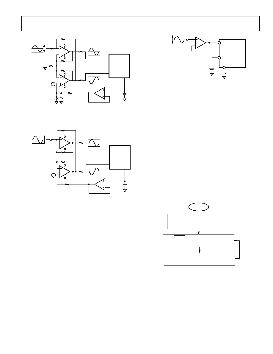
Figure 27. Dual Op Amp Circuit to Convert a Single-Ended
Bipolar Signal into a Unipolar Differential Signal
10k
VREF p-p
VREF
GND
440
220
27
V+
V–
V+
V–
A
VIN+
VIN–
VREF
AD7933/
AD7934
0.47F
03
71
3-
03
6
3.75V
2.5V
1.25V
3.75V
2.5V
1.25V
Figure 28. Dual Op Amp Circuit to Convert a Single-Ended Unipolar
Signal into a Differential Signal
Another method of driving the AD7933/AD7934 is to use the
AD8138 differential amplifier. The AD8138 can be used as a
single-ended-to-differential amplifier, or differential-to-differential
amplifier. The device is as easy to use as an op amp and greatly
simplifies differential signal amplification and driving.
Pseudo Differential Mode
The AD7933/AD7934 can have two pseudo differential pairs by
setting the MODE0 and MODE1 bits in the control register to 1
and 0, respectively. VIN+ is connected to the signal source and
must have an amplitude of VREF (or 2 × VREF depending on the
range chosen) to make use of the full dynamic range of the part.
A dc input is applied to the VIN pin. The voltage applied to this
input provides an offset from ground or a pseudo ground for
the VIN+ input. The benefit of pseudo differential inputs is that
they separate the analog input signal ground from the ADC
ground, allowing the cancellation of dc common-mode
voltages. Typically, this range can extend to 0.3 V to +0.7 V
shows a connection diagram for pseudo differential mode.
VIN+
VIN–
VREF
AD7933/
AD7934*
*ADDITIONAL PINS OMITTED FOR CLARITY.
VREF p-p
0.47F
DC INPUT
VOLTAGE
03
71
3-
03
7
+
Figure 29. Pseudo Differential Mode Connection Diagram
ANALOG INPUT SELECTION
As shown in Table 10, users can set up their analog input
configuration by setting the values in the MODE0 and MODE1
bits in the control register. Assuming the configuration has been
chosen, there are two different ways of selecting the analog
input to be converted depending on the state of the SEQ0 and
SEQ1 bits in the control register.
Traditional Multichannel Operation (SEQ0 = SEQ1 = 0)
Any one of four analog input channels or two pairs of channels
can be selected for conversion in any order by setting the SEQ0
and SEQ1 bits in the control register to 0. The channel to be
converted is selected by writing to the address bits, ADD1 and
ADD0, in the control register to program the multiplexer prior
to the conversion. This mode of operation is that of a traditional
multichannel ADC where each data write selects the next
channel for conversion. Figure 30 shows a flowchart of this
mode of operation. The channel configurations are shown in
POWER ON
WRITE TO THE CONTROL REGISTER TO
SET UP OPERATING MODE, ANALOG INPUT
AND OUTPUT CONFIGURATION
SET SEQ0 = SEQ1 = 0. SELECT THE DESIRED
CHANNEL TO CONVERT ON (ADD1 TO ADD0).
ISSUE CONVST PULSE TO INITIATE A CONVERSION
ON THE SELECTED CHANNEL.
INITIATE A READ CYCLE TO READ THE DATA
FROM THE SELECTED CHANNEL.
INITIATE A WRITE CYCLE TO SELECT THE NEXT
CHANNEL TO BE CONVERTED ON BY
CHANGING THE VALUES OF BITS ADD2 TO ADD0
IN THE CONTROL REGISTER. SEQ0 = SEQ1 = 0.
0
37
13
-0
38
Figure 30. Traditional Multichannel Operation Flow Chart
Using the Sequencer: Consecutive Sequence
(SEQ0 = 1, SEQ1 = 1)
A sequence of consecutive channels can be converted beginning
with Channel 0 and ending with a final channel selected by
writing to the ADD1 and ADD0 bits in the control register. This
is done by setting the SEQ0 and SEQ1 bits in the control
register both to 1. Once the control register is written to, the
next conversion is on Channel 0, then Channel 1, and so on
until the channel selected by the Address Bit ADD1 and Address
Bit ADD0 is reached. The ADC then returns to Channel 0 and
相关PDF资料 |
PDF描述 |
|---|---|
| MS3106F22-23S | CONN PLUG 8POS STRAIGHT W/SCKT |
| MS27467T11F99S | CONN PLUG 7POS STRAIGHT W/SCKT |
| SI8244CB-C-IS1 | IC AUDIO DRIVER PWM 16-SOIC |
| MS27467E9B44S | CONN PLUG 4POS STRAIGHT W/SCKT |
| SI8244BB-C-IS1 | IC AUDIO DRIVER PWM 16-SOIC |
相关代理商/技术参数 |
参数描述 |
|---|---|
| AD7937 | 制造商:AD 制造商全称:Analog Devices 功能描述:LC2MOS 8+4 Loading Dual 12-Bit DAC |
| AD7937AR | 功能描述:IC DAC 12BIT DUAL 8+4 24-SOIC RoHS:否 类别:集成电路 (IC) >> 数据采集 - 数模转换器 系列:- 标准包装:2,400 系列:- 设置时间:- 位数:18 数据接口:串行 转换器数目:3 电压电源:模拟和数字 功率耗散(最大):- 工作温度:-40°C ~ 85°C 安装类型:表面贴装 封装/外壳:36-TFBGA 供应商设备封装:36-TFBGA 包装:带卷 (TR) 输出数目和类型:* 采样率(每秒):* |
| AD7937AR-REEL | 功能描述:IC DAC 12BIT DUAL 8+4 24-SOIC RoHS:否 类别:集成电路 (IC) >> 数据采集 - 数模转换器 系列:- 标准包装:2,400 系列:- 设置时间:- 位数:18 数据接口:串行 转换器数目:3 电压电源:模拟和数字 功率耗散(最大):- 工作温度:-40°C ~ 85°C 安装类型:表面贴装 封装/外壳:36-TFBGA 供应商设备封装:36-TFBGA 包装:带卷 (TR) 输出数目和类型:* 采样率(每秒):* |
| AD7937AR-REEL7 | 制造商:Analog Devices 功能描述:DAC 2CH R-2R 12-BIT 24SOIC W - Tape and Reel |
| AD7937BR | 功能描述:IC DAC 12BIT DUAL 8+4 24-SOIC RoHS:否 类别:集成电路 (IC) >> 数据采集 - 数模转换器 系列:- 标准包装:2,400 系列:- 设置时间:- 位数:18 数据接口:串行 转换器数目:3 电压电源:模拟和数字 功率耗散(最大):- 工作温度:-40°C ~ 85°C 安装类型:表面贴装 封装/外壳:36-TFBGA 供应商设备封装:36-TFBGA 包装:带卷 (TR) 输出数目和类型:* 采样率(每秒):* |
发布紧急采购,3分钟左右您将得到回复。