- 您现在的位置:买卖IC网 > PDF目录10252 > AD7934BRUZ-REEL7 (Analog Devices Inc)IC ADC 12BIT 4CH 1.5MSPS 28TSSOP PDF资料下载
参数资料
| 型号: | AD7934BRUZ-REEL7 |
| 厂商: | Analog Devices Inc |
| 文件页数: | 15/32页 |
| 文件大小: | 0K |
| 描述: | IC ADC 12BIT 4CH 1.5MSPS 28TSSOP |
| 标准包装: | 1,000 |
| 位数: | 12 |
| 采样率(每秒): | 1.5M |
| 数据接口: | 并联 |
| 转换器数目: | 1 |
| 功率耗散(最大): | 13.5mW |
| 电压电源: | 单电源 |
| 工作温度: | -40°C ~ 85°C |
| 安装类型: | 表面贴装 |
| 封装/外壳: | 28-TSSOP(0.173",4.40mm 宽) |
| 供应商设备封装: | 28-TSSOP |
| 包装: | 带卷 (TR) |
| 输入数目和类型: | 4 个单端,单极;2 个差分,单极;2 个伪差分,单极 |
第1页第2页第3页第4页第5页第6页第7页第8页第9页第10页第11页第12页第13页第14页当前第15页第16页第17页第18页第19页第20页第21页第22页第23页第24页第25页第26页第27页第28页第29页第30页第31页第32页
AD7933/AD7934
Rev. B | Page 22 of 32
starts the sequence again. The WR input must be kept high to
ensure that the control register is not accidentally overwritten
and the sequence interrupted. This pattern continues until the
AD7933/AD7934 is written to. Figure 31 shows the flowchart of
the consecutive sequence mode.
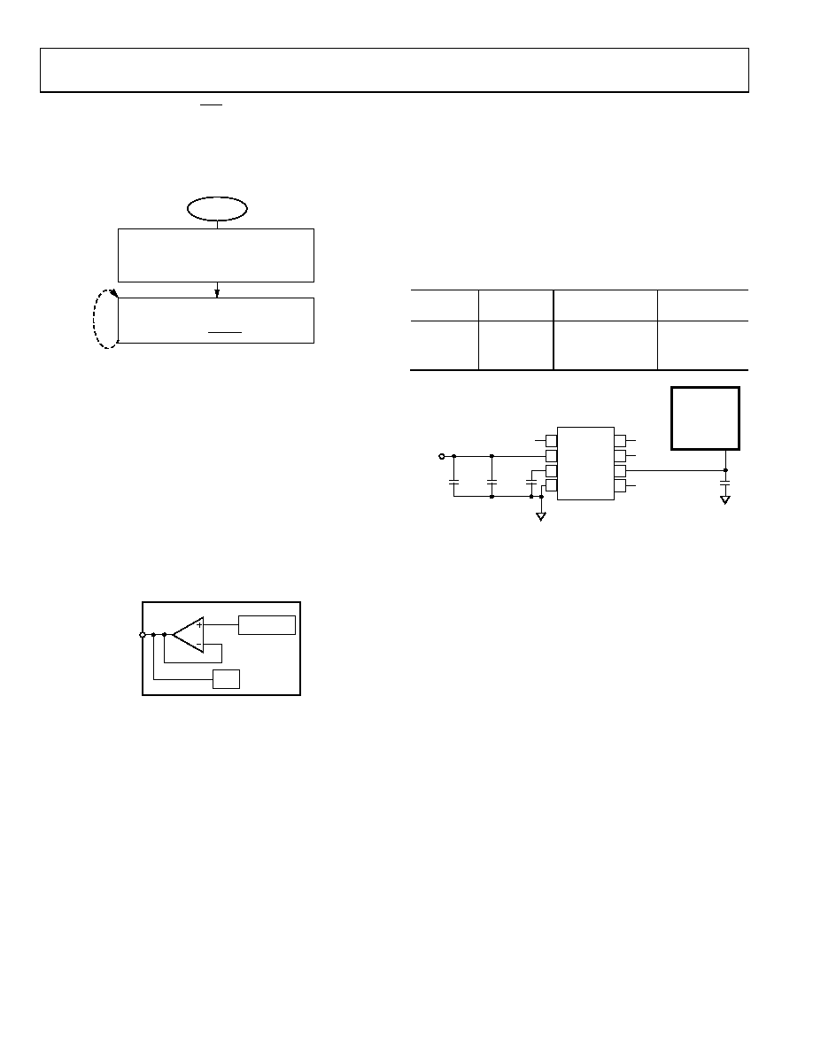
POWER ON
WRITE TO THE CONTROL REGISTER TO
SET UP OPERATING MODE, ANALOG INPUT
AND OUTPUT CONFIGURATION SELECT
FINAL CHANNEL (ADD1 AND ADD0) IN
CONSECUTIVE SEQUENCE.
SET SEQ0 = 1 SEQ1 = 1.
CONTINUOUSLY CONVERT ON A CONSECUTIVE
SEQUENCE OF CHANNELS FROM CHANNEL 0
UP TO AND INCLUDING THE PREVIOUSLY
SELECTED FINAL CHANNEL ON ADD1 AND ADD0
WITH EACH CONVST PULSE.
03
713
-039
Figure 31. Consecutive Sequence Mode Flow Chart
REFERENCE
The AD7933/AD7934 can operate with either the on-chip
reference or an external reference. The internal reference is
selected by setting the REF bit in the internal control register to 1.
A block diagram of the internal reference circuitry is shown in
Figure 32. The internal reference circuitry includes an on-chip
2.5 V band gap reference and a reference buffer. When using the
internal reference, decouple the VREFIN/VREFOUT pin to AGND with a
0.47 μF capacitor. This internal reference not only provides the
reference for the analog-to-digital conversion, but it can also be
used externally in the system. It is recommended that the
reference output is buffered using an external precision op amp
before applying it anywhere in the system.
REFERENCE
AD7933/
AD7934
ADC
BUFFER
VREFIN/
VREFOUT
03
713
-04
0
Figure 32. Internal Reference Circuit Block Diagram
Alternatively, an external reference can be applied to the
VREFIN/VREFOUT pin of the AD7933/AD7934. An external
reference input is selected by setting the REF bit in the internal
control register to 0. The external reference input range is 0.1 V
to VDD. It is important to ensure that, when choosing the
reference value, the maximum analog input range (VIN MAX) is
never greater than VDD + 0.3 V to comply with the maximum
ratings of the device. For example, if operating in differential
mode and the reference is sourced from VDD, the 0 V to 2 × VREF
range cannot be used. This is because the analog input signal
range now extends to 2 × VDD, which exceeds the maximum
rating conditions. In the pseudo differential modes, the user
must ensure that VREF + VIN ≤ VDD when using the 0 V to VREF
range, or when using the 2 × VREF range that 2 × VREF + VIN ≤ VDD.
In all cases, the specified reference is 2.5 V.
The performance of the part with different reference values is
shown in Figure 9 to Figure 11. The value of the reference sets
the analog input span and the common-mode voltage range.
Errors in the reference source result in gain errors in the
AD7933/AD7934 transfer function and add to the specified
full-scale errors on the part.
Table 12 lists suitable voltage references available from Analog
Devices that can be used. Figure 33 shows a typical connection
diagram for an external reference.
Table 12. Examples of Suitable Voltage References
Reference
Output
Voltage (V)
Initial Accuracy
(% maximum)
Operating
Current (μA)
2.5/3
0.04
1000
2.5
0.04
500
2.048
0.05
500
1
AD780
NC
8
2
+VIN
NC
7
3
GND
6
4
TEMP
5
O/P SELECT
TRIM
VOUT
VREF
2.5V
NC
VDD
NC = NO CONNECT
10nF
0.1F
*ADDITIONAL PINS OMITTED FOR CLARITY.
AD7933/
AD7934*
0
371
3-
0
41
Figure 33. Typical VREF Connection Diagram
Digital Inputs
The digital inputs applied to the AD7933/AD7934 are not
limited by the maximum ratings that limit the analog inputs.
Instead, the digital inputs applied can go to 7 V and are not
restricted by the VDD + 0.3 V limit that is on the analog inputs.
Another advantage of the digital inputs not being restricted by
the VDD + 0.3 V limit is the fact that power supply sequencing
issues are avoided. If any of these inputs are applied before VDD,
there is no risk of latch-up as there would be on the analog inputs
if a signal greater than 0.3 V was applied prior to VDD.
VDRIVE Input
The AD7933/AD7934 have a VDRIVE feature. VDRIVE controls the
voltage at which the parallel interface operates. VDRIVE allows the
ADC to easily interface to 3 V and 5 V processors.
For example, if the AD7933/AD7934 are operated with a VDD
of 5 V, and the VDRIVE pin is powered from a 3 V supply, the
AD7933/AD7934 have better dynamic performance with a
VDD of 5 V while still being able to interface to 3 V processors.
Ensure that VDRIVE does not exceed VDD by more than 0.3 V (see
the Absolute Maximum Ratings section).
相关PDF资料 |
PDF描述 |
|---|---|
| MS3106F22-23S | CONN PLUG 8POS STRAIGHT W/SCKT |
| MS27467T11F99S | CONN PLUG 7POS STRAIGHT W/SCKT |
| SI8244CB-C-IS1 | IC AUDIO DRIVER PWM 16-SOIC |
| MS27467E9B44S | CONN PLUG 4POS STRAIGHT W/SCKT |
| SI8244BB-C-IS1 | IC AUDIO DRIVER PWM 16-SOIC |
相关代理商/技术参数 |
参数描述 |
|---|---|
| AD7937 | 制造商:AD 制造商全称:Analog Devices 功能描述:LC2MOS 8+4 Loading Dual 12-Bit DAC |
| AD7937AR | 功能描述:IC DAC 12BIT DUAL 8+4 24-SOIC RoHS:否 类别:集成电路 (IC) >> 数据采集 - 数模转换器 系列:- 标准包装:2,400 系列:- 设置时间:- 位数:18 数据接口:串行 转换器数目:3 电压电源:模拟和数字 功率耗散(最大):- 工作温度:-40°C ~ 85°C 安装类型:表面贴装 封装/外壳:36-TFBGA 供应商设备封装:36-TFBGA 包装:带卷 (TR) 输出数目和类型:* 采样率(每秒):* |
| AD7937AR-REEL | 功能描述:IC DAC 12BIT DUAL 8+4 24-SOIC RoHS:否 类别:集成电路 (IC) >> 数据采集 - 数模转换器 系列:- 标准包装:2,400 系列:- 设置时间:- 位数:18 数据接口:串行 转换器数目:3 电压电源:模拟和数字 功率耗散(最大):- 工作温度:-40°C ~ 85°C 安装类型:表面贴装 封装/外壳:36-TFBGA 供应商设备封装:36-TFBGA 包装:带卷 (TR) 输出数目和类型:* 采样率(每秒):* |
| AD7937AR-REEL7 | 制造商:Analog Devices 功能描述:DAC 2CH R-2R 12-BIT 24SOIC W - Tape and Reel |
| AD7937BR | 功能描述:IC DAC 12BIT DUAL 8+4 24-SOIC RoHS:否 类别:集成电路 (IC) >> 数据采集 - 数模转换器 系列:- 标准包装:2,400 系列:- 设置时间:- 位数:18 数据接口:串行 转换器数目:3 电压电源:模拟和数字 功率耗散(最大):- 工作温度:-40°C ~ 85°C 安装类型:表面贴装 封装/外壳:36-TFBGA 供应商设备封装:36-TFBGA 包装:带卷 (TR) 输出数目和类型:* 采样率(每秒):* |
发布紧急采购,3分钟左右您将得到回复。