- 您现在的位置:买卖IC网 > PDF目录10252 > AD7934BRUZ-REEL7 (Analog Devices Inc)IC ADC 12BIT 4CH 1.5MSPS 28TSSOP PDF资料下载
参数资料
| 型号: | AD7934BRUZ-REEL7 |
| 厂商: | Analog Devices Inc |
| 文件页数: | 20/32页 |
| 文件大小: | 0K |
| 描述: | IC ADC 12BIT 4CH 1.5MSPS 28TSSOP |
| 标准包装: | 1,000 |
| 位数: | 12 |
| 采样率(每秒): | 1.5M |
| 数据接口: | 并联 |
| 转换器数目: | 1 |
| 功率耗散(最大): | 13.5mW |
| 电压电源: | 单电源 |
| 工作温度: | -40°C ~ 85°C |
| 安装类型: | 表面贴装 |
| 封装/外壳: | 28-TSSOP(0.173",4.40mm 宽) |
| 供应商设备封装: | 28-TSSOP |
| 包装: | 带卷 (TR) |
| 输入数目和类型: | 4 个单端,单极;2 个差分,单极;2 个伪差分,单极 |
第1页第2页第3页第4页第5页第6页第7页第8页第9页第10页第11页第12页第13页第14页第15页第16页第17页第18页第19页当前第20页第21页第22页第23页第24页第25页第26页第27页第28页第29页第30页第31页第32页
AD7933/AD7934
Rev. B | Page 27 of 32
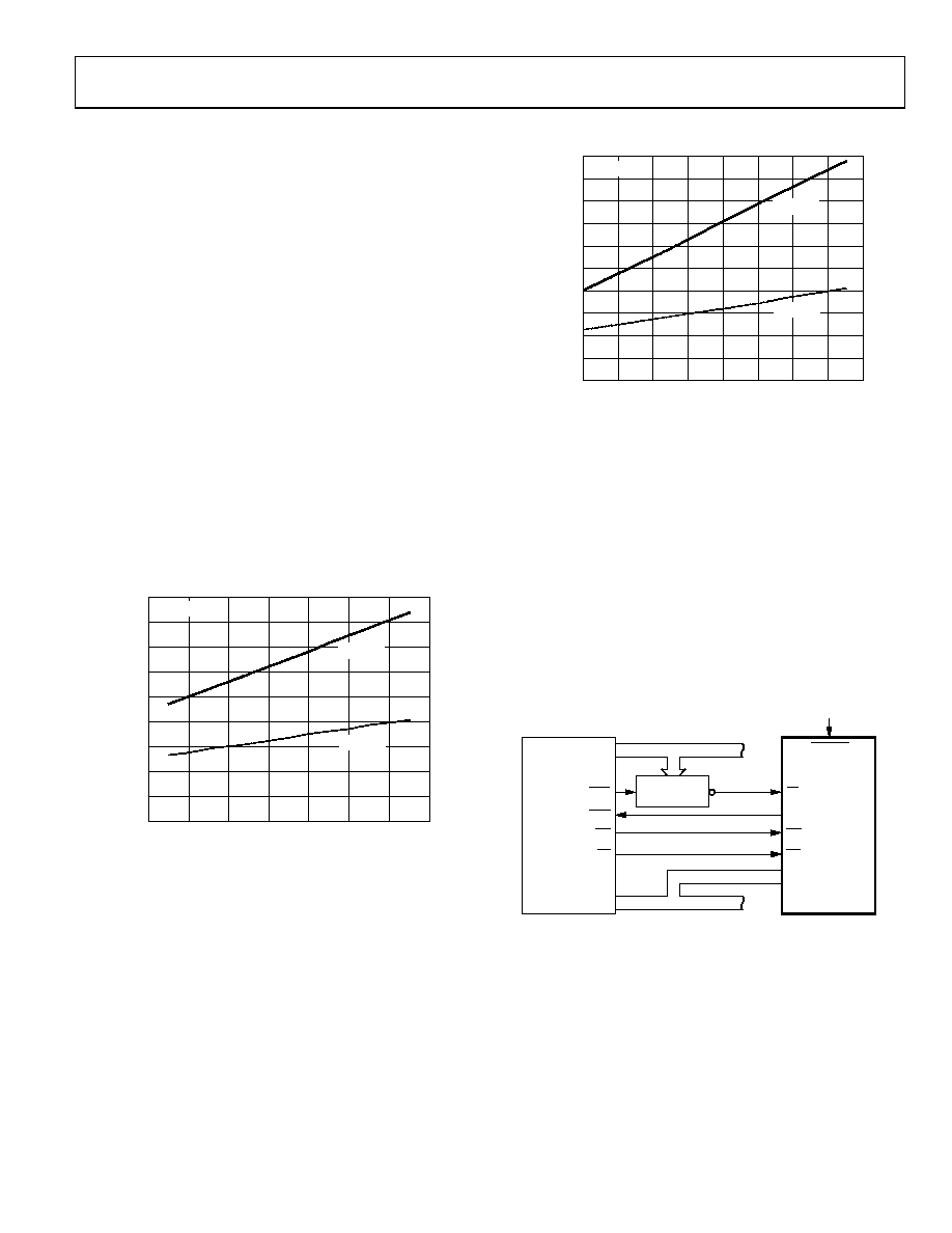
POWER vs. THROUGHPUT RATE
A considerable advantage of powering the ADC down after a
conversion is that the power consumption of the part is
significantly reduced at lower throughput rates. When using the
different power modes, the AD7933/AD7934 are only powered
up for the duration of the conversion. Therefore, the average
power consumption per cycle is significantly reduced. Figure 39
shows a plot of power vs. throughput rate when operating in
autostandby mode for both VDD = 5 V and 3 V. For example, if
the device runs at a throughput rate of 10 kSPS, the overall cycle
time is 100 μs. If the maximum CLKIN frequency of 25.5 MHz
is used, the conversion time accounts for only 0.525 μs of the
overall cycle time while the AD7933/AD7934 remains in
standby mode for the remainder of the cycle.
Figure 40 shows a plot of the power vs. the throughput rate
when operating in normal mode for both VDD = 5 V and 3 V.
In both plots, the figures apply when using the internal
reference. If an external reference is used, the power-up time
reduces to 600 ns; therefore, the AD7933/AD7934 remains in
standby for a greater time in every cycle. Additionally, the
current consumption, when converting, should be lower than
the specified maximum of 2.7 mA with VDD = 5 V, or 2.0 mA
with VDD = 3 V, respectively.
THROUGHPUT (kSPS)
P
O
WE
R
(
m
W)
1.8
0.8
1.0
1.2
1.4
1.6
0
0.6
0.4
0.2
0
20
406080
100
120
140
TA = 25°C
VDD =5V
VDD =3V
03
71
3-
0
42
Figure 39. Power vs. Throughput in
Autostandby Mode Using Internal Reference
THROUGHPUT (kSPS)
P
O
WE
R
(
m
W)
10
4
5
6
7
8
9
0
3
2
1
0
200
400
600
800
1000
1200
1600
1400
TA = 25°C
VDD =5V
VDD =3V
03
71
3-
0
43
Figure 40. Power vs. Throughput in Normal Mode Using Internal Reference
MICROPROCESSOR INTERFACING
AD7933/AD7934 to ADSP-21xx Interface
Figure 41 shows the AD7933/AD7934 interfaced to the
ADSP-21xx series of DSPs as a memory-mapped device.
A single wait state may be necessary to interface the AD7933/
AD7934 to the ADSP-21xx, depending on the clock speed of
the DSP. The wait state can be programmed via the data memory
wait state control register of the ADSP-21xx (see the ADSP-21xx
family User’s Manual for details). The following instruction
reads from the AD7933/AD7934:
MR = DM (ADC)
where ADC is the address of the AD7933/AD7934.
AD7933/
AD7934*
ADSP-21xx*
WR
RD
DB0 TO DB11
D0 TO D23
A0 TO A15
DMS
IRQ2
BUSY
CS
CONVST
DSP/USER SYSTEM
WR
RD
*ADDITIONAL PINS OMITTED FOR CLARITY.
ADDRESS BUS
DATA BUS
ADDRESS
DECODER
03
71
3-
0
44
Figure 41. Interfacing to the ADSP-21xx
相关PDF资料 |
PDF描述 |
|---|---|
| MS3106F22-23S | CONN PLUG 8POS STRAIGHT W/SCKT |
| MS27467T11F99S | CONN PLUG 7POS STRAIGHT W/SCKT |
| SI8244CB-C-IS1 | IC AUDIO DRIVER PWM 16-SOIC |
| MS27467E9B44S | CONN PLUG 4POS STRAIGHT W/SCKT |
| SI8244BB-C-IS1 | IC AUDIO DRIVER PWM 16-SOIC |
相关代理商/技术参数 |
参数描述 |
|---|---|
| AD7937 | 制造商:AD 制造商全称:Analog Devices 功能描述:LC2MOS 8+4 Loading Dual 12-Bit DAC |
| AD7937AR | 功能描述:IC DAC 12BIT DUAL 8+4 24-SOIC RoHS:否 类别:集成电路 (IC) >> 数据采集 - 数模转换器 系列:- 标准包装:2,400 系列:- 设置时间:- 位数:18 数据接口:串行 转换器数目:3 电压电源:模拟和数字 功率耗散(最大):- 工作温度:-40°C ~ 85°C 安装类型:表面贴装 封装/外壳:36-TFBGA 供应商设备封装:36-TFBGA 包装:带卷 (TR) 输出数目和类型:* 采样率(每秒):* |
| AD7937AR-REEL | 功能描述:IC DAC 12BIT DUAL 8+4 24-SOIC RoHS:否 类别:集成电路 (IC) >> 数据采集 - 数模转换器 系列:- 标准包装:2,400 系列:- 设置时间:- 位数:18 数据接口:串行 转换器数目:3 电压电源:模拟和数字 功率耗散(最大):- 工作温度:-40°C ~ 85°C 安装类型:表面贴装 封装/外壳:36-TFBGA 供应商设备封装:36-TFBGA 包装:带卷 (TR) 输出数目和类型:* 采样率(每秒):* |
| AD7937AR-REEL7 | 制造商:Analog Devices 功能描述:DAC 2CH R-2R 12-BIT 24SOIC W - Tape and Reel |
| AD7937BR | 功能描述:IC DAC 12BIT DUAL 8+4 24-SOIC RoHS:否 类别:集成电路 (IC) >> 数据采集 - 数模转换器 系列:- 标准包装:2,400 系列:- 设置时间:- 位数:18 数据接口:串行 转换器数目:3 电压电源:模拟和数字 功率耗散(最大):- 工作温度:-40°C ~ 85°C 安装类型:表面贴装 封装/外壳:36-TFBGA 供应商设备封装:36-TFBGA 包装:带卷 (TR) 输出数目和类型:* 采样率(每秒):* |
发布紧急采购,3分钟左右您将得到回复。