- 您现在的位置:买卖IC网 > PDF目录10664 > AD7980BCPZ-RL7 (Analog Devices Inc)IC ADC 16BIT 1MSPS SAR 10LFCSP PDF资料下载
参数资料
| 型号: | AD7980BCPZ-RL7 |
| 厂商: | Analog Devices Inc |
| 文件页数: | 8/28页 |
| 文件大小: | 0K |
| 描述: | IC ADC 16BIT 1MSPS SAR 10LFCSP |
| 标准包装: | 1 |
| 系列: | PulSAR® |
| 位数: | 16 |
| 采样率(每秒): | 1M |
| 数据接口: | DSP,MICROWIRE?,QSPI?,串行,SPI? |
| 转换器数目: | 1 |
| 功率耗散(最大): | 9mW |
| 电压电源: | 单电源 |
| 工作温度: | -40°C ~ 125°C |
| 安装类型: | 表面贴装 |
| 封装/外壳: | 10-WFDFN 裸露焊盘,CSP |
| 供应商设备封装: | 10-LFCSP-WD(3x3) |
| 包装: | 标准包装 |
| 输入数目和类型: | 1 个伪差分,单极 |
| 其它名称: | AD7980BCPZ-RL7DKR |
第1页第2页第3页第4页第5页第6页第7页当前第8页第9页第10页第11页第12页第13页第14页第15页第16页第17页第18页第19页第20页第21页第22页第23页第24页第25页第26页第27页第28页
AD7980
Data Sheet
Rev. C | Page 16 of 28
VOLTAGE REFERENCE INPUT
The AD7980 voltage reference input, REF, has a dynamic input
impedance and should therefore be driven by a low impedance
source with efficient decoupling between the REF and GND
pins, as explained in the Layout section.
When REF is driven by a very low impedance source, for example,
chip capacitor is appropriate for optimum performance.
If an unbuffered reference voltage is used, the decoupling value
depends on the reference used. For instance, a 22 F (X5R,
1206 size) ceramic chip capacitor is appropriate for optimum
performance using a low temperature drift ADR43x reference.
If desired, a reference-decoupling capacitor value as small as
2.2 F can be used with a minimal impact on performance,
especially DNL.
Regardless, there is no need for an additional lower value ceramic
decoupling capacitor (for example, 100 nF) between the REF
and GND pins.
POWER SUPPLY
The AD7980 uses two power supply pins: a core supply, VDD, and
a digital input/output interface supply, VIO. VIO allows direct
interface with any logic between 1.8 V and 5.0 V. To reduce the
number of supplies needed, VIO and VDD can be tied together.
The AD7980 is independent of power supply sequencing between
VIO and VDD. Additionally, it is very insensitive to power supply
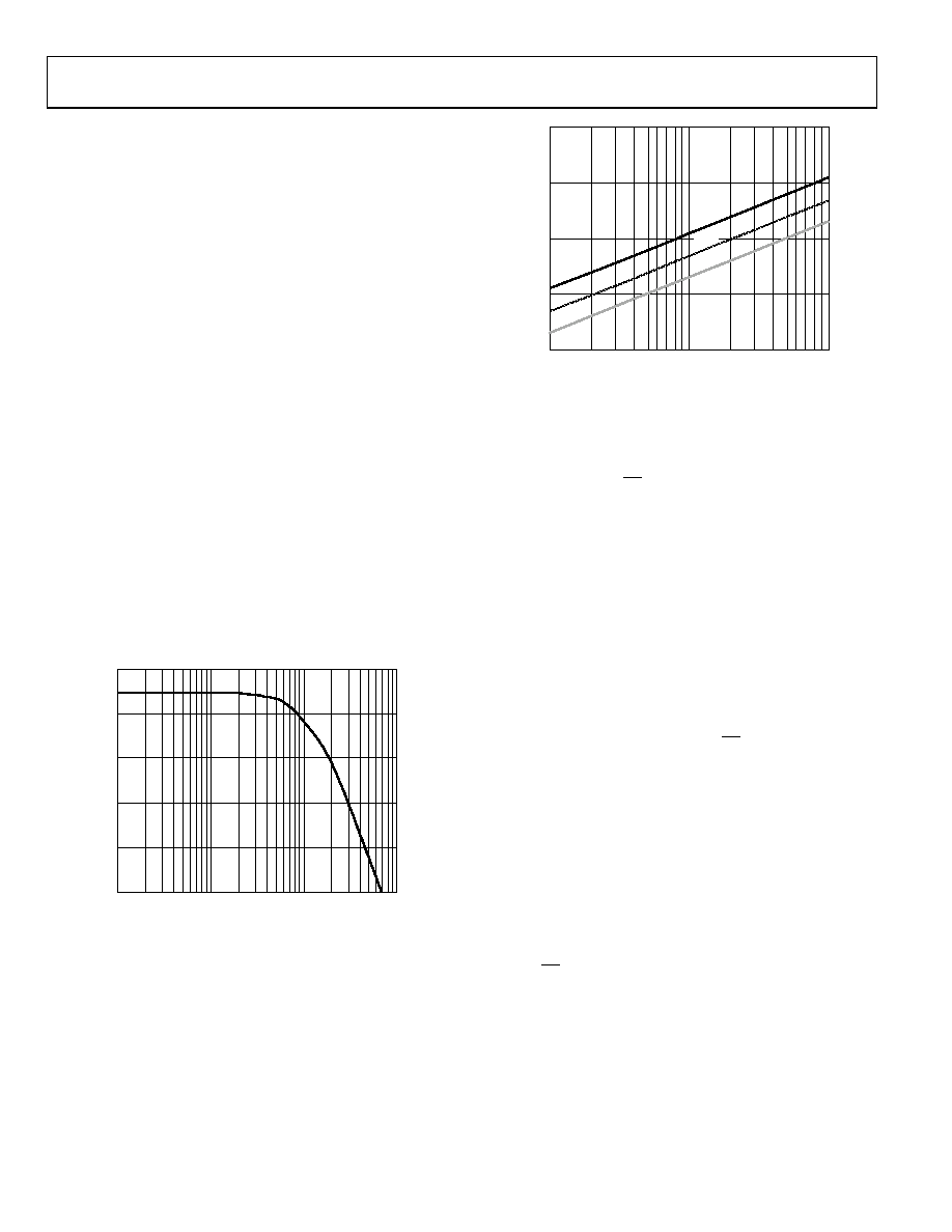
variations over a wide frequency range, as shown in Figure 29.
80
55
1
1000
06392-
062
FREQUENCY (kHz)
P
S
RR
(
d
B)
10
100
75
70
65
60
Figure 29. PSRR vs. Frequency
To ensure optimum performance, VDD should be roughly half
of REF, the voltage reference input. For example, if REF is 5.0 V,
VDD should be set to 2.5 V (±5%).
The AD7980 powers down automatically at the end of each
conversion phase and, therefore, the power scales linearly with
the sampling rate. This makes the part ideal for low sampling
rate (even of a few Hz) and low battery-powered applications.
06392-
055
10.000
1.000
0.100
0.010
0.001
O
PER
A
T
ING
CURRE
NT
S
(
mA)
100000
SAMPLING RATE (SPS)
10000
1000000
IVDD
IVIO
IREF
Figure 30. Operating Currents vs. Sampling Rate
DIGITAL INTERFACE
Though the AD7980 has a reduced number of pins, it offers
flexibility in its serial interface modes.
The AD7980, when in CS mode, is compatible with SPI, QSPI,
and digital hosts. This interface can use either a 3-wire or 4-wire
interface. A 3-wire interface using the CNV, SCK, and SDO
signals minimizes wiring connections useful, for instance, in
isolated applications. A 4-wire interface using the SDI, CNV,
SCK, and SDO signals allows CNV, which initiates the
conversions, to be independent of the readback timing (SDI).
This is useful in low jitter sampling or simultaneous sampling
applications.
The AD7980, when in chain mode, provides a daisy-chain
feature using the SDI input for cascading multiple ADCs on a
single data line similar to a shift register.
The mode in which the part operates depends on the SDI level
when the CNV rising edge occurs. The CS mode is selected if
SDI is high, and the chain mode is selected if SDI is low. The
SDI hold time is such that when SDI and CNV are connected
together, the chain mode is selected.
In either mode, the AD7980 offers the flexibility to optionally
force a start bit in front of the data bits. This start bit can be
used as a busy signal indicator to interrupt the digital host and
trigger the data reading. Otherwise, without a busy indicator,
the user must time out the maximum conversion time prior to
readback.
The busy indicator feature is enabled
In the CS mode if CNV or SDI is low when the ADC
conversion ends (see Figure 34 and Figure 38).
In the chain mode if SCK is high during the CNV rising edge
相关PDF资料 |
PDF描述 |
|---|---|
| VE-J1N-MW-F4 | CONVERTER MOD DC/DC 18.5V 100W |
| MAX9646EBS+TG45 | IC COMPARATOR W/REF 4UCSP |
| MAX3086CSD+T | IC TXRX RS485/422 10MBPS 14-SOIC |
| MAX9645EUK+T | IC COMPARATOR W/REF SOT23-5 |
| VE-J1N-MW-F2 | CONVERTER MOD DC/DC 18.5V 100W |
相关代理商/技术参数 |
参数描述 |
|---|---|
| AD7980BRMZ | 功能描述:ADC 16BIT 1MSPS 1.25LSB 10-MSOP RoHS:是 类别:集成电路 (IC) >> 数据采集 - 模数转换器 系列:PulSAR® 标准包装:1 系列:microPOWER™ 位数:8 采样率(每秒):1M 数据接口:串行,SPI? 转换器数目:1 功率耗散(最大):- 电压电源:模拟和数字 工作温度:-40°C ~ 125°C 安装类型:表面贴装 封装/外壳:24-VFQFN 裸露焊盘 供应商设备封装:24-VQFN 裸露焊盘(4x4) 包装:Digi-Reel® 输入数目和类型:8 个单端,单极 产品目录页面:892 (CN2011-ZH PDF) 其它名称:296-25851-6 |
| AD7980BRMZRL7 | 功能描述:ADC 16BIT 1MSPS LP 10-MSOP RoHS:是 类别:集成电路 (IC) >> 数据采集 - 模数转换器 系列:PulSAR® 标准包装:1,000 系列:- 位数:12 采样率(每秒):300k 数据接口:并联 转换器数目:1 功率耗散(最大):75mW 电压电源:单电源 工作温度:0°C ~ 70°C 安装类型:表面贴装 封装/外壳:24-SOIC(0.295",7.50mm 宽) 供应商设备封装:24-SOIC 包装:带卷 (TR) 输入数目和类型:1 个单端,单极;1 个单端,双极 |
| AD7980-EP | 制造商:AD 制造商全称:Analog Devices 功能描述:16-Bit, 1 MSPS PulSAR ADC in MSOP QFN |
| AD7980SRMZ-EP | 制造商:Analog Devices 功能描述:16-BIT, 1 MSPS PULSAR ADC IN MSOP/QFN - Rail/Tube |
| AD7980SRMZ-EP-RL7 | 制造商:Rochester Electronics LLC 功能描述: 制造商:Analog Devices 功能描述:ADC 16BIT 1MSPS LP 10-MSOP 制造商:Analog Devices 功能描述:CONVERTER - ADC |
发布紧急采购,3分钟左右您将得到回复。