参数资料
| 型号: | AD8105ABPZ |
| 厂商: | Analog Devices Inc |
| 文件页数: | 21/36页 |
| 文件大小: | 0K |
| 描述: | IC CROSSPOINT SWIT 32X16 304BGA |
| 标准包装: | 1 |
| 功能: | 交叉点开关 |
| 电路: | 1 x 32:16 |
| 电压电源: | 单/双电源 |
| 电压 - 电源,单路/双路(±): | 4.5 V ~ 5.5 V,±2.5V |
| 电流 - 电源: | 340mA |
| 工作温度: | -40°C ~ 85°C |
| 安装类型: | 表面贴装 |
| 封装/外壳: | 304-BGA 裸露焊盘 |
| 供应商设备封装: | 304-BGA(31x31) |
| 包装: | 托盘 |
第1页第2页第3页第4页第5页第6页第7页第8页第9页第10页第11页第12页第13页第14页第15页第16页第17页第18页第19页第20页当前第21页第22页第23页第24页第25页第26页第27页第28页第29页第30页第31页第32页第33页第34页第35页第36页
AD8104/AD8105
Rev. 0 | Page 28 of 36
When operating with a differential input, care must be taken to
keep the common mode, or average, of the input voltages within
the linear operating range of the AD8104/AD8105 receiver. This
common-mode range can extend rail-to-rail, provided the
differential signal swing is small enough to avoid forward
biasing the ESD diodes (it is safest to keep the common mode
plus differential signal excursions within the supply voltages
of the part). See the Specifications section for guaranteed
input range.
The differential output of the AD8104/AD8105 receiver is
linear for a peak of 1.4 V of output voltage difference (1.4 V
peak input difference for the AD8104, and 0.7 V peak input
difference for the AD8105). Taking the output differentially,
using the two output phases, this allows 2.8 V p-p of linear
output signal swing. Beyond this level, the signal path can
saturate and limits the signal swing. This is not a desired
operation, as the supply current increases and the signal path is
slow to recover from clipping. The absolute maximum allowed
differential input signal is limited by the long-term reliability of
the input stage. The limits in the Absolute Maximum Ratings
section should be observed in order to avoid degrading device
performance permanently.
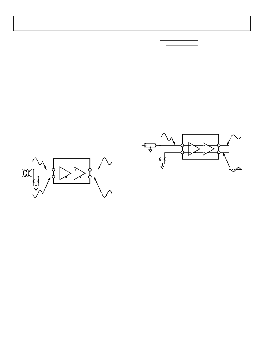
RCVR
AD8104
OPn
ONn
IPn
INn
50
06
61
2-
06
6
Figure 66. Example of Input Driven Differentially
Single-Ended Input
The AD8104/AD8105 input receivers can be driven single-
endedly (unbalanced). From the standpoint of the receiver,
there is very little difference between signals applied positive
and negative in two phases to the input pair vs. a signal applied
to one input only with the other input held at a constant
potential. One small difference is that the common mode
between the input pins is changing if only one input is moving,
and there is a very small common-mode to differential
conversion gain in the receiver that adds an additional gain
error to the output (see the common-mode rejection ratio for
the input stage in the Specifications section). For low
frequencies, this gain error is negligible. The common-mode
rejection ratio degrades with increasing frequency.
When operating the AD8104/AD8105 receivers single-endedly,
the observed input resistance at each input pin is lower than in
the differential input case, due to a fraction of the receiver
internal output voltage appearing as a common-mode signal on
its input terminals, bootstrapping the voltage on the input
resistance. This single-ended input resistance can be calculated
by the equation
)
(
2
1
F
S
G
F
S
G
IN
R
+
×
+
=
where:
RG = 2.5 kΩ.
RS is the user single-ended source resistance (such as 37.5 Ω for
a back-terminated 75 Ω source).
RF = 2.538 kΩ for the AD8104 and 5.075 kΩ for the AD8105.
In most cases, a single-ended input signal is referred to midsup-
ply, typically ground. In this case, the undriven differential input
can be connected to ground. For best dynamic performance and
lowest offset voltage, this unused input should be terminated
with an impedance matching the driven input, instead of being
directly shorted to ground. Due to the differential feedback of
the receiver, there is high frequency signal current in the
undriven input and it should be treated as a signal line in the
board design.
RCVR
OPn
ONn
IPn
INn
75
(OR 37.5)
AD8104
06
61
2-
0
67
Figure 67. Example of Input Driven Single-Ended
AC Coupling of Inputs
It is possible to ac couple the inputs of the AD8104/AD8105
receiver. This is simplified because the bias current does not
need to be supplied externally. A capacitor in series with the
inputs to the AD8104/AD8105 creates a high-pass filter with
the input impedance of the device. This capacitor needs to be
sized such that the corner frequency is low enough for
frequencies of interest.
Differential Output
Benefits of Differential Operation
The AD8104/AD8105 have a fully differential switch core, with
differential outputs. The two output voltages move in opposite
polarity, with a differential feedback loop maintaining a fixed
output stage differential gain of +1 (the different overall signal
path gains between the AD8104 and AD8105 are set in the
input stage for best signal-to-noise ratio). This differential
output stage provides a benefit of crosstalk-canceling due to
parasitic coupling from one output to another being equal and
out of phase. Additionally, if the output of the device is utilized
in a differential design, noise, crosstalk, and offset voltages
generated on-chip that are coupled equally into both outputs are
cancelled by the common-mode rejection ratio of the next
device in the signal chain. By utilizing the AD8104/AD8105
outputs in a differential application, the best possible noise and
offset specifications can be realized.
相关PDF资料 |
PDF描述 |
|---|---|
| AD8107ASTZ | IC CROSSPOINT SWITCH 16X5 80LQFP |
| AD8108ASTZ | IC VIDEO CROSSPOINT SWIT 80LQFP |
| AD8110ASTZ | IC VIDEO CROSSPOINT SWIT 80LQFP |
| AD8112JSTZ | IC CROSSPOINT SWIT 16X8 100LQFP |
| AD8113JSTZ | IC VIDEO CROSSPOINT SWIT 100LQFP |
相关代理商/技术参数 |
参数描述 |
|---|---|
| AD8106 | 制造商:AD 制造商全称:Analog Devices 功能描述:260 MHz, 16 】 5 Buffered Video Crosspoint Switches |
| AD8106ASTZ | 功能描述:IC CROSSPOINT SWITCH 16X5 80LQFP RoHS:是 类别:集成电路 (IC) >> 接口 - 模拟开关,多路复用器,多路分解器 系列:- 其它有关文件:STG4159 View All Specifications 标准包装:5,000 系列:- 功能:开关 电路:1 x SPDT 导通状态电阻:300 毫欧 电压电源:双电源 电压 - 电源,单路/双路(±):±1.65 V ~ 4.8 V 电流 - 电源:50nA 工作温度:-40°C ~ 85°C 安装类型:表面贴装 封装/外壳:7-WFBGA,FCBGA 供应商设备封装:7-覆晶 包装:带卷 (TR) |
| AD8106-EB | 制造商:AD 制造商全称:Analog Devices 功能描述:260 MHz, 16 】 5 Buffered Video Crosspoint Switches |
| AD8107 | 制造商:AD 制造商全称:Analog Devices 功能描述:260 MHz, 16 】 5 Buffered Video Crosspoint Switches |
| AD8107ASTZ | 功能描述:IC CROSSPOINT SWITCH 16X5 80LQFP RoHS:是 类别:集成电路 (IC) >> 接口 - 模拟开关,多路复用器,多路分解器 系列:- 其它有关文件:STG4159 View All Specifications 标准包装:5,000 系列:- 功能:开关 电路:1 x SPDT 导通状态电阻:300 毫欧 电压电源:双电源 电压 - 电源,单路/双路(±):±1.65 V ~ 4.8 V 电流 - 电源:50nA 工作温度:-40°C ~ 85°C 安装类型:表面贴装 封装/外壳:7-WFBGA,FCBGA 供应商设备封装:7-覆晶 包装:带卷 (TR) |
发布紧急采购,3分钟左右您将得到回复。