参数资料
| 型号: | AD8105ABPZ |
| 厂商: | Analog Devices Inc |
| 文件页数: | 25/36页 |
| 文件大小: | 0K |
| 描述: | IC CROSSPOINT SWIT 32X16 304BGA |
| 标准包装: | 1 |
| 功能: | 交叉点开关 |
| 电路: | 1 x 32:16 |
| 电压电源: | 单/双电源 |
| 电压 - 电源,单路/双路(±): | 4.5 V ~ 5.5 V,±2.5V |
| 电流 - 电源: | 340mA |
| 工作温度: | -40°C ~ 85°C |
| 安装类型: | 表面贴装 |
| 封装/外壳: | 304-BGA 裸露焊盘 |
| 供应商设备封装: | 304-BGA(31x31) |
| 包装: | 托盘 |
第1页第2页第3页第4页第5页第6页第7页第8页第9页第10页第11页第12页第13页第14页第15页第16页第17页第18页第19页第20页第21页第22页第23页第24页当前第25页第26页第27页第28页第29页第30页第31页第32页第33页第34页第35页第36页
AD8104/AD8105
Rev. 0 | Page 31 of 36
operation as well, as there is a common-mode-to-differential
gain conversion that becomes greater at higher frequencies.
During operation of the AD8104/AD8105, transient currents
flow into the VOCM net from the amplifier control loops.
Although the magnitude of these currents are small (10 μA to
20 μA per output), they can contribute to crosstalk if they flow
through significant impedances. Driving VOCM with a low
impedance, low noise source is desirable.
Power Dissipation
Calculation of Power Dissipation
8
4
15
85
MA
X
IMU
M
P
O
W
E
R
(W
)
AMBIENT TEMPERATURE (°C)
TJ = 150°C
7
6
5
25
35
45
55
65
75
06
61
2-
0
70
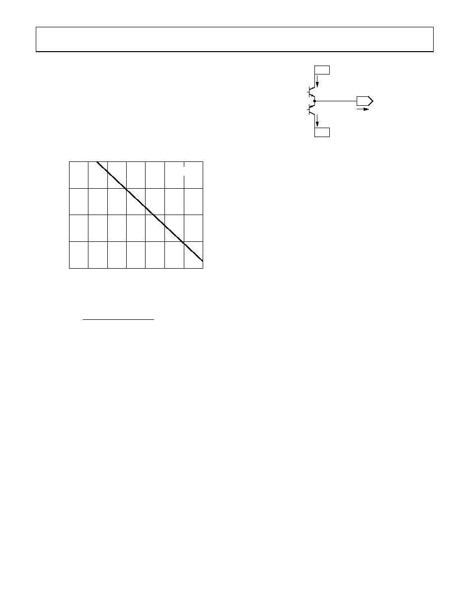
Figure 70. Maximum Die Power Dissipation vs. Ambient Temperature
The curve in Figure 70 was calculated from
JA
AMBIENT
MAX
JUNCTION
MAX
D
T
P
θ
=
,
(1)
As an example, if the AD8104/AD8105 is enclosed in an envi-
ronment at 45°C (TA), the total on-chip dissipation under all
load and supply conditions must not be allowed to exceed 7.0 W.
When calculating on-chip power dissipation, it is necessary to
include the rms current being delivered to the load, multiplied
by the rms voltage drop on the AD8104/AD8105 output
devices. For a sinusoidal output, the on-chip power dissipation
due to the load can be approximated by
(
)
RMS
OUTPUT
RMS
UTPUT
O
POS
OUTPUT
D
I
V
P
,
×
=
For nonsinusoidal output, the power dissipation should be
calculated by integrating the on-chip voltage drop multiplied by
the load current over one period.
The user can subtract the quiescent current for the Class AB
output stage when calculating the loaded power dissipation. For
each output stage driving a load, subtract a quiescent power
according to
(
)
QUIESCENT
OUTPUT
NEG
POS
OUTPUT
DQ
I
V
P
,
×
=
where
IOUTPUT, QUIESCENT = 1.65 mA for each single-ended output pin.
For each disabled output, the quiescent power supply current in
VPOS and VNEG drops by approximately 9 mA.
QNPN
QPNP
VNEG
VPOS
VOUTPUT
IOUTPUT
IOUTPUT, QUIESCENT
06
61
2-
0
71
Figure 71. Simplified Output Stage
Example
For the AD8104/AD8105, in an ambient temperature of 85°C,
with all 16 outputs driving 1 V rms into 100 Ω loads and power
supplies at ±2.5 V, follow these steps:
1.
Calculate power dissipation of AD8104/AD8105 using data
sheet quiescent currents. Disregard VDD current, as it is
insignificant.
(
) (
)
VNEG
NEG
VPOS
POS
QUIESCENT
D
I
V
I
V
P
×
+
×
=
,
(
) (
)
W
7
.
1
mA
340
V
5
.
2
mA
340
V
5
.
2
,
=
×
+
×
=
QUIESCENT
D
P
2.
Calculate power dissipation from loads. For a differential
output and ground-referenced load, the output power is
symmetrical in each output phase.
(
)
RMS
OUTPUT
RMS
OUTPUT
POS
OUTPUT
D
I
V
P
,
×
=
(
)
()
mW
15
Ω
100
/
V
1
V
1
V
5
.
2
,
=
×
=
OUTPUT
D
P
There are 16 output pairs, or 32 output currents.
W
48
.
0
mW
15
32
,
=
×
=
OUTPUT
D
nP
3.
Subtract the quiescent output stage current for number of
loads (32 in this example). The output stage is either
standing, or driving a load, but the current only needs to
be counted once (valid for output voltages > 0.5 V).
(
)
QUIESCENT
OUTPUT
NEG
POS
OUTPUT
DQ
I
V
P
,
×
=
(
)
mW
25
.
8
mA
65
.
1
V)
5
.
2
(
V
5
.
2
,
=
×
=
OUTPUT
DQ
P
There are 16 output pairs, or 32 output currents.
W
26
.
0
mW
25
.
8
32
,
=
×
=
OUTPUT
DQ
nP
4.
Verify that the power dissipation does not exceed the
maximum allowed value.
OUTPUT
DQ
OUTPUT
D
QUIESCENT
D
CHIP
ON
D
nP
P
,
+
=
W
9
.
1
W
26
.
0
W
48
.
0
W
7
.
1
,
=
+
=
CHIP
ON
D
P
From Figure 70 or Equation 1, this power dissipation is below
the maximum allowed dissipation for all ambient temperatures
up to and including 85°C.
相关PDF资料 |
PDF描述 |
|---|---|
| AD8107ASTZ | IC CROSSPOINT SWITCH 16X5 80LQFP |
| AD8108ASTZ | IC VIDEO CROSSPOINT SWIT 80LQFP |
| AD8110ASTZ | IC VIDEO CROSSPOINT SWIT 80LQFP |
| AD8112JSTZ | IC CROSSPOINT SWIT 16X8 100LQFP |
| AD8113JSTZ | IC VIDEO CROSSPOINT SWIT 100LQFP |
相关代理商/技术参数 |
参数描述 |
|---|---|
| AD8106 | 制造商:AD 制造商全称:Analog Devices 功能描述:260 MHz, 16 】 5 Buffered Video Crosspoint Switches |
| AD8106ASTZ | 功能描述:IC CROSSPOINT SWITCH 16X5 80LQFP RoHS:是 类别:集成电路 (IC) >> 接口 - 模拟开关,多路复用器,多路分解器 系列:- 其它有关文件:STG4159 View All Specifications 标准包装:5,000 系列:- 功能:开关 电路:1 x SPDT 导通状态电阻:300 毫欧 电压电源:双电源 电压 - 电源,单路/双路(±):±1.65 V ~ 4.8 V 电流 - 电源:50nA 工作温度:-40°C ~ 85°C 安装类型:表面贴装 封装/外壳:7-WFBGA,FCBGA 供应商设备封装:7-覆晶 包装:带卷 (TR) |
| AD8106-EB | 制造商:AD 制造商全称:Analog Devices 功能描述:260 MHz, 16 】 5 Buffered Video Crosspoint Switches |
| AD8107 | 制造商:AD 制造商全称:Analog Devices 功能描述:260 MHz, 16 】 5 Buffered Video Crosspoint Switches |
| AD8107ASTZ | 功能描述:IC CROSSPOINT SWITCH 16X5 80LQFP RoHS:是 类别:集成电路 (IC) >> 接口 - 模拟开关,多路复用器,多路分解器 系列:- 其它有关文件:STG4159 View All Specifications 标准包装:5,000 系列:- 功能:开关 电路:1 x SPDT 导通状态电阻:300 毫欧 电压电源:双电源 电压 - 电源,单路/双路(±):±1.65 V ~ 4.8 V 电流 - 电源:50nA 工作温度:-40°C ~ 85°C 安装类型:表面贴装 封装/外壳:7-WFBGA,FCBGA 供应商设备封装:7-覆晶 包装:带卷 (TR) |
发布紧急采购,3分钟左右您将得到回复。