参数资料
| 型号: | AD8105ABPZ |
| 厂商: | Analog Devices Inc |
| 文件页数: | 29/36页 |
| 文件大小: | 0K |
| 描述: | IC CROSSPOINT SWIT 32X16 304BGA |
| 标准包装: | 1 |
| 功能: | 交叉点开关 |
| 电路: | 1 x 32:16 |
| 电压电源: | 单/双电源 |
| 电压 - 电源,单路/双路(±): | 4.5 V ~ 5.5 V,±2.5V |
| 电流 - 电源: | 340mA |
| 工作温度: | -40°C ~ 85°C |
| 安装类型: | 表面贴装 |
| 封装/外壳: | 304-BGA 裸露焊盘 |
| 供应商设备封装: | 304-BGA(31x31) |
| 包装: | 托盘 |
第1页第2页第3页第4页第5页第6页第7页第8页第9页第10页第11页第12页第13页第14页第15页第16页第17页第18页第19页第20页第21页第22页第23页第24页第25页第26页第27页第28页当前第29页第30页第31页第32页第33页第34页第35页第36页
AD8104/AD8105
Rev. 0 | Page 35 of 36
If multiple AD8104/AD8105s are to be driven in parallel, a fly-
by input termination scheme is very useful, but the distance
from each AD8104/AD8105 input to the driven input transmis-
sion line is a stub that should be minimized in length and
parasitics using the discussed guidelines.
When driving the AD8104/AD8105 single-endedly, the
undriven input is often terminated with a resistance to balance
the input stage. It can be seen that by terminating the undriven
input with a resistor of one half the characteristic impedance,
the input stage is perfectly balanced (37.5 Ω, for example, to
balance the two parallel 75 Ω terminations on the driven input).
However, due to the feedback in the input receiver, there is high
speed signal current leaving the undriven input. To terminate
this high speed signal, proper transmission line techniques
should be used. One solution is to adjust the trace width to
create a transmission line of half the characteristic impedance
and terminate the far end with this resistance (37.5 Ω in a 75 Ω
system). This is not often practical as trace widths become large.
In most cases, the best practical solution is to place the half-
characteristic impedance resistor as close as possible (preferably
less than 1.5 cm away) and to reduce the parasitics of the stub
(by removing the ground plane under the stub, for example).
In either case, the designer must decide if the layout complexity
created by a balanced, terminated solution is preferable to
simply grounding the undriven input at the ball with no trace.
Although the examples discussed so far are for input termina-
tion, the theory is similar for output back-termination. Taking
the AD8104/AD8105 as an ideal voltage source, any distance of
routing between the AD8104/AD8105 and a back-termination
resistor will be an impedance mismatch that potentially creates
reflections. For this reason, back-termination resistors should
also be placed close to the AD8104/AD8105. In practice,
because back-termination resistors are series elements, they
can be placed close to the AD8104/AD8105 outputs.
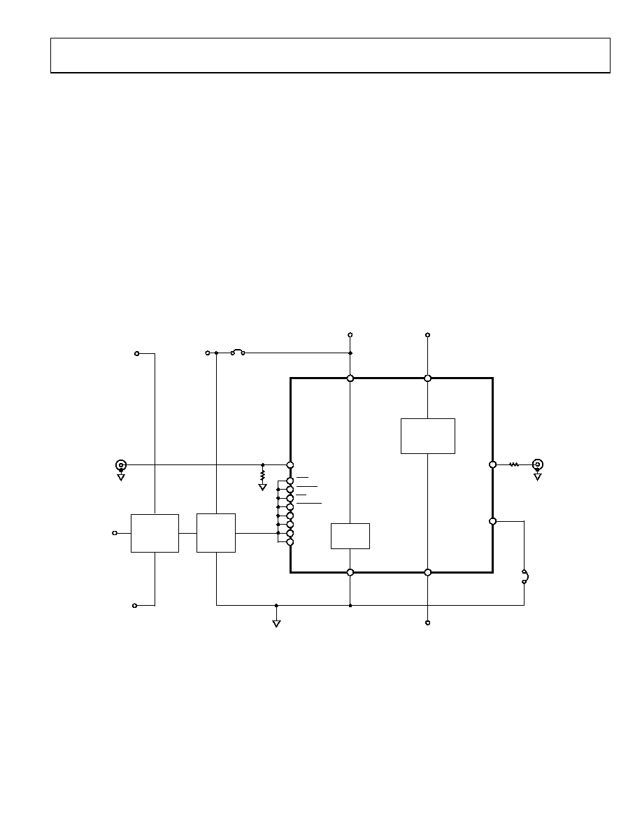
GND
VOCM
VDD
AD8104/
AD8105
ON[15:0], OP[15:0]
IN[31:0], IP[31:0]
CLK
RESET
WE
UPDATE
DATA IN
DATA OUT
J3
PLD_VDD
PC_VDD
PC_GND
SMA
VPOS
VNEG
DGND
VDD
VPOS
VNEG
CPLD
50
LOGIC
PC
PARALLEL
PORT
IN[31:0],
IP[31:0]
LOGIC
ISOLATORS
J8,
W3 TO W7
D0 TO D5
A0 TO A3
ON[15:0],
OP[15:0]
ANALOG
06
61
2-
0
73
Figure 73. Evaluation Board Simplified Schematic
相关PDF资料 |
PDF描述 |
|---|---|
| AD8107ASTZ | IC CROSSPOINT SWITCH 16X5 80LQFP |
| AD8108ASTZ | IC VIDEO CROSSPOINT SWIT 80LQFP |
| AD8110ASTZ | IC VIDEO CROSSPOINT SWIT 80LQFP |
| AD8112JSTZ | IC CROSSPOINT SWIT 16X8 100LQFP |
| AD8113JSTZ | IC VIDEO CROSSPOINT SWIT 100LQFP |
相关代理商/技术参数 |
参数描述 |
|---|---|
| AD8106 | 制造商:AD 制造商全称:Analog Devices 功能描述:260 MHz, 16 】 5 Buffered Video Crosspoint Switches |
| AD8106ASTZ | 功能描述:IC CROSSPOINT SWITCH 16X5 80LQFP RoHS:是 类别:集成电路 (IC) >> 接口 - 模拟开关,多路复用器,多路分解器 系列:- 其它有关文件:STG4159 View All Specifications 标准包装:5,000 系列:- 功能:开关 电路:1 x SPDT 导通状态电阻:300 毫欧 电压电源:双电源 电压 - 电源,单路/双路(±):±1.65 V ~ 4.8 V 电流 - 电源:50nA 工作温度:-40°C ~ 85°C 安装类型:表面贴装 封装/外壳:7-WFBGA,FCBGA 供应商设备封装:7-覆晶 包装:带卷 (TR) |
| AD8106-EB | 制造商:AD 制造商全称:Analog Devices 功能描述:260 MHz, 16 】 5 Buffered Video Crosspoint Switches |
| AD8107 | 制造商:AD 制造商全称:Analog Devices 功能描述:260 MHz, 16 】 5 Buffered Video Crosspoint Switches |
| AD8107ASTZ | 功能描述:IC CROSSPOINT SWITCH 16X5 80LQFP RoHS:是 类别:集成电路 (IC) >> 接口 - 模拟开关,多路复用器,多路分解器 系列:- 其它有关文件:STG4159 View All Specifications 标准包装:5,000 系列:- 功能:开关 电路:1 x SPDT 导通状态电阻:300 毫欧 电压电源:双电源 电压 - 电源,单路/双路(±):±1.65 V ~ 4.8 V 电流 - 电源:50nA 工作温度:-40°C ~ 85°C 安装类型:表面贴装 封装/外壳:7-WFBGA,FCBGA 供应商设备封装:7-覆晶 包装:带卷 (TR) |
发布紧急采购,3分钟左右您将得到回复。