参数资料
| 型号: | AD8330ARQZ-RL |
| 厂商: | Analog Devices Inc |
| 文件页数: | 10/32页 |
| 文件大小: | 0K |
| 描述: | IC AMP VGA 150MHZ LN LP 16QSOP |
| 标准包装: | 2,500 |
| 放大器类型: | 可变增益 |
| 电路数: | 1 |
| 输出类型: | 差分,满摆幅 |
| 转换速率: | 1500 V/µs |
| -3db带宽: | 150MHz |
| 电流 - 输入偏压: | 100nA |
| 电流 - 电源: | 20mA |
| 电压 - 电源,单路/双路(±): | 2.7 V ~ 6 V |
| 工作温度: | -40°C ~ 85°C |
| 安装类型: | 表面贴装 |
| 封装/外壳: | 16-SSOP(0.154",3.90mm 宽) |
| 供应商设备封装: | 16-QSOP |
| 包装: | 带卷 (TR) |
| 配用: | AD8330-EVALZ-ND - BOARD EVAL FOR AD8330 |
第1页第2页第3页第4页第5页第6页第7页第8页第9页当前第10页第11页第12页第13页第14页第15页第16页第17页第18页第19页第20页第21页第22页第23页第24页第25页第26页第27页第28页第29页第30页第31页第32页
AD8330
Data Sheet
Rev. F | Page 18 of 32
VGAIN (V)
80
0.001
1
N
O
ISE
(n
V/
√Hz
)
G
AI
N
(
d
B)
–40
–60
–20
0
20
40
60
10
100
1k
10k
100k
0.01
0.1
1
10
03217-
053
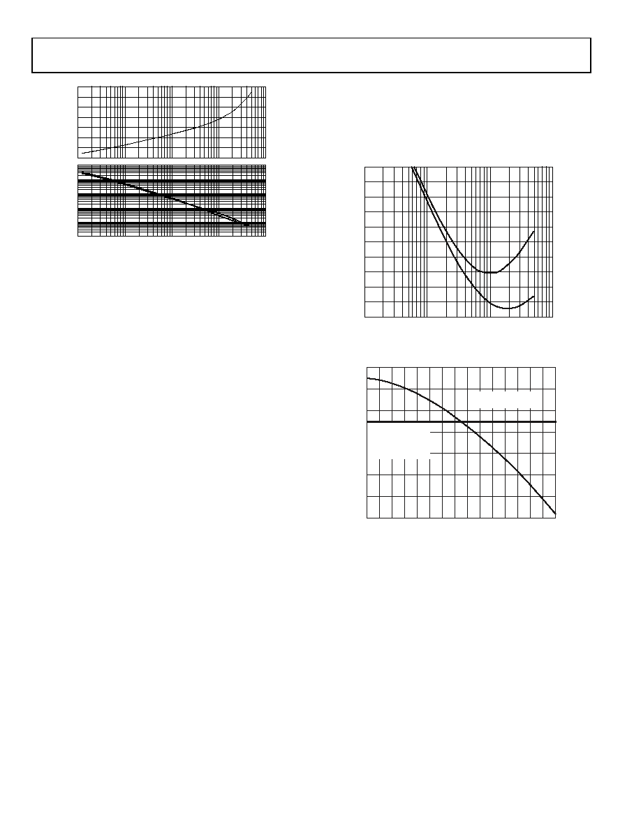
Figure 52. Gain Control Function and Input Referred Noise Spectral Density
over a 120 dB Range
Noise, Input Capacity, and Dynamic Range
The design of variable gain amplifiers invariably incurs some
compromises in noise performance. However, the structure of
the AD8330 is such that this penalty is minimal. Examination
of the simplified schematic (Figure 47) shows that the input
voltage is converted to current-mode form by the two 500
resistors at Pin INHI and Pin INLO, whose combined Johnson
noise contributes 4.08 nV/√Hz. The total input noise at full
gain, when driven from a low impedance source, is typically
5 nV/√Hz after accounting for the voltage and current noise
contributions of the loop amplifier. For a 200 kHz channel
bandwidth, this amounts to 2.24 μV rms. The peak input at full
gain is ±6.4 mV, or +4.5 mV rms for a sine wave signal. The
signal-to-noise ratio at full input, that is, the dynamic range, for
these conditions is, thus, 20 log10(4.5 mV/2.24 μV), or 66 dB.
The value of VMAG has essentially no effect on the input referred
noise, but it is assumed to be 0.5 V.
Below midgain (25 dB, VDBS = 0.75 V), noise in the output
section dominates, and the total input noise is 11 nV/√Hz, or
4.9 V rms in a 200 kHz bandwidth, and the peak input is
78 mV rms. Thus, the dynamic range increases to 84 dB.
At minimum gain, the input noise is up to 120 nV/√Hz, or
53.7 mV rms in the assumed 200 kHz bandwidth, while the
input capacity is ±2 V, or +1.414 V rms (sine), a dynamic range
of 88.4 dB. In calculating the dynamic range for other channel
bandwidths, f, subtract 10 log10(f/200 kHz) from these
illustrative values. A system operating with a 2 MHz bandwidth,
for example, exhibits dynamic range values that are uniformly
10 dB lower; used in an audio application with a 20 kHz band-
width, they are 10 dB higher.
Noise figure is a misleading metric for amplifiers that are not
impedance matched at their input, which is the special condi-
tion resulting only when both the voltage and current components
of a signal, that is, the signal power, are used at the input port.
When a source of impedance (RS) is terminated using a resistor
of RS (a condition that is not to be confused with matching),
only one of these components is used, either the current (as in
the AD8330) or the voltage. Then, even if the amplifier is
perfect, the noise figure cannot be better than 3 dB. The 1 k
internal termination resistance would result in a minimum
noise figure of 3 dB for an RS of 1 k if the amplifier were
noise-free. However, this is not the case, and the minimum
noise figure occurs at a slightly different value of RS (for an
example, see Figure 53 and the Using the AD8330 section).
RS ()
10k
100
10
1k
15
14
13
12
11
10
9
8
7
5
6
N
OIS
E
FIGU
R
E
03217-
054
Figure 53. Noise Figure for Source Resistance of 50 to 5 k, at f = 10 MHz
(Lower) and 100 MHz (Simulation)
VDBS (V)
0
0.1
DY
NAM
IC
RANG
E
(
d
B/
√Hz
)
0.2 0.3 0.4 0.5 0.6 0.7 0.8 0.9 1.0 1.1 1.2 1.3 1.4 1.5
144
132
128
124
120
140
136
116
CONSTANT 1V rms
OUTPUT, BOTH CASES
X-AMP WITH 40dB
OF GAIN AND AN
INPUT NSD
OF nV/
√Hz
03217-
055
Figure 54. Dynamic Range in dB/√Hz vs. VDBS (VMAG = 0.5 V, 1 V rms Output)
Compared with a Representative X-AMP (Simulation)
Dynamic Range
The ratio of peak output swing, expressed in rms terms, to the
output-referred noise spectral density provides a measure of
dynamic range, in dB/√Hz. For a certain class of variable gain
amplifiers, exemplified by the Analog Devices X-AMP family,
the dynamic range is essentially independent of the gain setting
because the peak output swing and noise are both constant. The
AD8330 provides a different dynamic range profile because
there is no longer a constant relationship between these two
parameters. Figure 54 compares the dynamic range of the
AD8330 to a representative X-AMP.
Input Common-Mode Range and Rejection Ratio
Input Pin INHI and Pin INLO should be ac-coupled in most
applications to achieve the stated noise performance. In general,
when direct coupling is used, care must be taken in setting the
dc voltage level at these inputs, and particularly when minimizing
相关PDF资料 |
PDF描述 |
|---|---|
| 3-1445055-1 | CONN HEADER 3MM 11POS R/A TIN |
| 2020-42T-ALF | GAS DISCHARGE TUBE 3 POLE 360V |
| 170M5265 | FUSE 900A 690V 2KN/110 AR UC |
| AD713JRZ-16-REEL | IC OPAMP BIFET QUAD PREC 16SOIC |
| 77313-118-40LF | BERGSTIK |
相关代理商/技术参数 |
参数描述 |
|---|---|
| AD8330-EVAL | 制造商:AD 制造商全称:Analog Devices 功能描述:Low Cost, DC to 150 MHz Variable Gain Amplifier |
| AD8330-EVALZ | 功能描述:BOARD EVAL FOR AD8330 RoHS:是 类别:编程器,开发系统 >> 评估板 - 运算放大器 系列:- 产品培训模块:Lead (SnPb) Finish for COTS Obsolescence Mitigation Program 标准包装:1 系列:- |
| AD8331 | 制造商:AD 制造商全称:Analog Devices 功能描述:Ultralow Noise VGAs with Preamplifier and Programmable RIN |
| AD8331_06 | 制造商:AD 制造商全称:Analog Devices 功能描述:Ultralow Noise VGAs with Preamplifier and Programmable RIN |
| AD8331_10 | 制造商:AD 制造商全称:Analog Devices 功能描述:Ultralow Noise VGAs with Preamplifier and Programmable RIN |
发布紧急采购,3分钟左右您将得到回复。