参数资料
| 型号: | AD8330ARQZ-RL |
| 厂商: | Analog Devices Inc |
| 文件页数: | 9/32页 |
| 文件大小: | 0K |
| 描述: | IC AMP VGA 150MHZ LN LP 16QSOP |
| 标准包装: | 2,500 |
| 放大器类型: | 可变增益 |
| 电路数: | 1 |
| 输出类型: | 差分,满摆幅 |
| 转换速率: | 1500 V/µs |
| -3db带宽: | 150MHz |
| 电流 - 输入偏压: | 100nA |
| 电流 - 电源: | 20mA |
| 电压 - 电源,单路/双路(±): | 2.7 V ~ 6 V |
| 工作温度: | -40°C ~ 85°C |
| 安装类型: | 表面贴装 |
| 封装/外壳: | 16-SSOP(0.154",3.90mm 宽) |
| 供应商设备封装: | 16-QSOP |
| 包装: | 带卷 (TR) |
| 配用: | AD8330-EVALZ-ND - BOARD EVAL FOR AD8330 |
第1页第2页第3页第4页第5页第6页第7页第8页当前第9页第10页第11页第12页第13页第14页第15页第16页第17页第18页第19页第20页第21页第22页第23页第24页第25页第26页第27页第28页第29页第30页第31页第32页
Data Sheet
AD8330
Rev. F | Page 17 of 32
VIN
VMAG
TIME (ns)
0.10
–400
–300
–200
–100
0
100
200
300
0.05
0
–0.05
–0.10
1.2
1.0
0.8
0.6
0.4
0.2
0
2.5
2.0
1.5
1.0
0.5
0
–0.5
–1.0
–1.5
–2.0
VOUT
03
21
7
-05
1
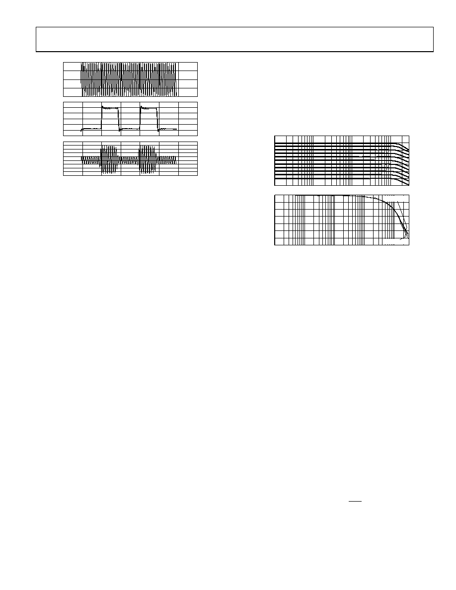
Figure 50. Using VMAG in Modulation Mode
Another gain related feature allows both gain control ranges
to be accurately raised by 200 mV. To enable this offset, open
circuit CMGN (Pin 6, LFCSP; Pin 8, LQFP) and add a 0.1 μF
capacitor to ground. In use, the nominal range for VDBS extends
from 0.2 V to 1.7 V and VMAG from 0.2 V to 5.2 V. These
specifications apply for any supply voltage. This allows the use
of DACs whose output range does not include ground as sources
for the gain control function(s).
Note that the 200 mV that appears on this pin affects the
response to an externally applied VMAG, but when Pin VMAG is
unconnected, the internally set default value of 0.5 V still applies.
Furthermore, Pin CMGN can, if desired, be driven by a user-
supplied voltage to reposition the baseline for VDBS (or for an
externally applied VMAG) to any other voltage up to 500 mV. In
all cases, the gain scaling, its law conformance, and temperature
stability are unaffected.
Two Classes of Variable Gain Amplifiers
Note that there are two broad classes of VGAs. The first type is
designed to cope with a very wide range of input amplitudes
and, by virtue of its gain control function, compress this range
down to an essentially constant output. This is the function
needed in an AGC system. Such a VGA is called an IVGA,
referring to a structure optimized to address a wide range of
input amplitudes. By contrast, an OVGA is optimized to deliver
a wide range of output values while operating with an essentially
constant input amplitude. This function might be needed, for
example, in providing a variable drive to a power amplifier.
It is apparent from the foregoing sections that the AD8330 is
both an IVGA and an OVGA in one package. This is an unusual
and possibly confusing degree of versatility for a VGA; therefore,
these two distinct control functions are described at separate
points throughout this data sheet to explain the operation and
applications of this product. It is, nevertheless, useful to briefly
describe the capabilities of these features when used together.
Amplitude/Phase Response
The ac response of the AD8330 is remarkably consistent not
only over the full 50 dB of its basic gain range, but also with
changes of gain due to alteration of VMAG, as demonstrated in
Figure 51. This is an overlay of two sets of results: first, with a
very low VMAG of 16 mV that reduces the overall gain by 30 dB
[20 × log10(500 mV/16 mV)]; second, with VMAG = 5 V that
increases the gain by 20 dB = 20 × log10(5 V/0.5 V).
FREQUENCY (Hz)
90
100k
10k
GA
IN
(
d
B
)
30
–10
–350
50
10
–30
1M
10M
100M
300M
70
P
H
A
S
E
(
D
e
g
rees
)
–50
–100
–150
–200
–250
–300
0
G = +70dB
G = –20dB
100k
1M
10M
100M 300M
03
21
7-
05
2
Figure 51. AC Performance over a 100 dB Gain Range Obtained by
Using Two Values of VMAG
This 50 dB step change in gain produces two sets of gain curves,
having a total gain span of 100 dB. It is apparent that the ampli-
tude and phase response are essentially independent of the gain
over this wide range, an aspect of the AD8330 performance
potential unprecedented in any prior VGA.
It is unusual for an application to require such a wide range of
gains; and, as a practical matter, the peak output voltage for
VMAG = 16 mV is reduced by the factor 16/500, compared to its
nominal value of ±2 V, to only ±64 mV. As previously noted,
most applications of VGAs require that they operate in a mode
that is predominantly of either an IVGA or OVGA style, rather
than mixed modes.
With this limitation in mind, and simply to illustrate the
unusual possibilities afforded by the AD8330, note that, with
appropriate drive to VDBS and VMAG in tandem, the gain span is a
remarkable 120 dB, extending from 50 dB to +70 dB, as shown
in Figure 52 for operation at 1 MHz and 100 MHz. In this case,
VDBS and VMAG are driven from a common control voltage,
VGAIN, that varies from 1.2 mV to 5 V, with 30% (1.5/5) of VGAIN
applied to VDBS, and 100% applied to VMAG.
The gain varies in a linear-in-dB manner with VDBS, although
the response from VMAG is linear-in-magnitude. Consequently, the
overall numerical gain as the product of these two functions is
V
6
.
0
10
3
.
0
V
5
.
0
/
GAIN
V
GAIN
V
GAIN
(7)
In rare cases where such a wide gain range is of value, the
calibration is still accurate and the temperature is stable.
相关PDF资料 |
PDF描述 |
|---|---|
| 3-1445055-1 | CONN HEADER 3MM 11POS R/A TIN |
| 2020-42T-ALF | GAS DISCHARGE TUBE 3 POLE 360V |
| 170M5265 | FUSE 900A 690V 2KN/110 AR UC |
| AD713JRZ-16-REEL | IC OPAMP BIFET QUAD PREC 16SOIC |
| 77313-118-40LF | BERGSTIK |
相关代理商/技术参数 |
参数描述 |
|---|---|
| AD8330-EVAL | 制造商:AD 制造商全称:Analog Devices 功能描述:Low Cost, DC to 150 MHz Variable Gain Amplifier |
| AD8330-EVALZ | 功能描述:BOARD EVAL FOR AD8330 RoHS:是 类别:编程器,开发系统 >> 评估板 - 运算放大器 系列:- 产品培训模块:Lead (SnPb) Finish for COTS Obsolescence Mitigation Program 标准包装:1 系列:- |
| AD8331 | 制造商:AD 制造商全称:Analog Devices 功能描述:Ultralow Noise VGAs with Preamplifier and Programmable RIN |
| AD8331_06 | 制造商:AD 制造商全称:Analog Devices 功能描述:Ultralow Noise VGAs with Preamplifier and Programmable RIN |
| AD8331_10 | 制造商:AD 制造商全称:Analog Devices 功能描述:Ultralow Noise VGAs with Preamplifier and Programmable RIN |
发布紧急采购,3分钟左右您将得到回复。