参数资料
| 型号: | AD8330ARQZ-RL |
| 厂商: | Analog Devices Inc |
| 文件页数: | 13/32页 |
| 文件大小: | 0K |
| 描述: | IC AMP VGA 150MHZ LN LP 16QSOP |
| 标准包装: | 2,500 |
| 放大器类型: | 可变增益 |
| 电路数: | 1 |
| 输出类型: | 差分,满摆幅 |
| 转换速率: | 1500 V/µs |
| -3db带宽: | 150MHz |
| 电流 - 输入偏压: | 100nA |
| 电流 - 电源: | 20mA |
| 电压 - 电源,单路/双路(±): | 2.7 V ~ 6 V |
| 工作温度: | -40°C ~ 85°C |
| 安装类型: | 表面贴装 |
| 封装/外壳: | 16-SSOP(0.154",3.90mm 宽) |
| 供应商设备封装: | 16-QSOP |
| 包装: | 带卷 (TR) |
| 配用: | AD8330-EVALZ-ND - BOARD EVAL FOR AD8330 |
第1页第2页第3页第4页第5页第6页第7页第8页第9页第10页第11页第12页当前第13页第14页第15页第16页第17页第18页第19页第20页第21页第22页第23页第24页第25页第26页第27页第28页第29页第30页第31页第32页
AD8330
Data Sheet
Rev. F | Page 20 of 32
Thus, when RL = 150 Ω, the gain is reduced by 6 dB; for
RL = 75 Ω, the reduction is 9.5 dB; and for RL = 50 Ω, it is 12 dB.
Gain Errors Due to On-Chip Resistor Tolerances
In all cases where external resistors are used, keep in mind that
all on-chip resistances, including the RO and the input resistance
(RI), are subject to variances of up to ±20%.
These variances need to be accounted for when calculating the
gain with input and output loading. This sensitivity can be avoided
by adjusting the source and load resistances to bear an inverse
relationship as follows:
If RS = αRI, then make RL = RO/α; or,
if RL = αRO, then make RS = RI/α
The simplest case is when RS = 1 kΩ and RL = 150 Ω, therefore,
the gain is 12 dB lower than the basic value. The reduction of
peak swing at the load can be corrected by using VMAG = 1 V,
thereby restoring 6 dB of gain; using VMAG = 2 V restores the full
basic gain and doubles the peak available output swing.
Output (Input) Common-Mode Control
The output voltages are nominally positioned at the midpoint of
the supply, VS/2, over the range 2.7 V < VS < 6 V, and this voltage
appears at Pin CNTR, which is not normally expected to be
loaded (the source resistance is ~4 kΩ). However, some circum-
stances require a small change in this voltage, and a resistor
from CNTR to ground can lower this voltage, whereas a resistor
to the supply raises it. On the other hand, this pin can be driven
by an external voltage source to set the common-mode level to
satisfy, for example, the needs of a following ADC. Any value
from 0.5 V above ground to 0.5 V below the supply is permissible.
Of course, when using an extreme common-mode level, the
available output swing is limited, and it is recommended that
a value equal or close to the default of VCNTR = VS/2 be used.
There may be a few millivolts of offset between the applied
voltage and the actual common-mode level at the output pins.
The input common-mode voltage, VCMI, at Pin INHI and
Pin INLO is slaved to the output. It bears a y = mx + b linear
and offset relationship to VCNTR as shown in Equation 14 where
y = VCMI, m = 0.757, x = VCNTR, and b = 1.12 V.
VCMI = 0.757 VCNTR + 1.12 V
(for VDBS = 0.75 V and T = 25°C)
(14)
The effects of VDBS and ambient temperature on VCMI are shown
T = 25°C and VS = 5 V is 3.01 V.
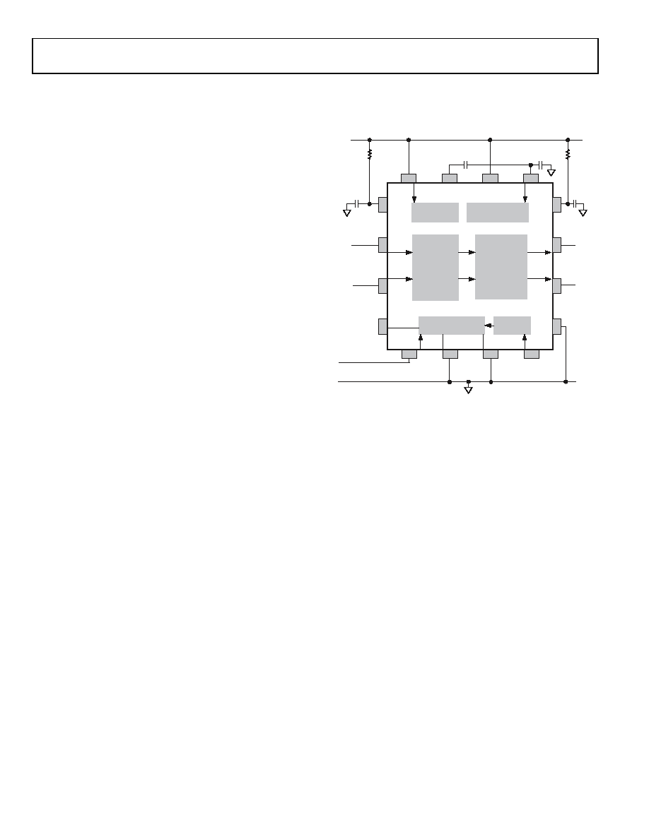
USING THE AD8330
This section describes a few general aspects of using the
AD8330. Applying the AD8330 to a wide variety of circum-
stances requires very few precautions.
As in all high frequency circuits, careful observation of the
ground nodes associated with each function is important. Three
positive supply pins are provided: VPSI supports the input cir-
cuitry that often operates at a relatively high sensitivity; VPOS
supports general bias sources and needs no decoupling; and
VPSO biases the output stage where decoupling can be useful in
maintaining a glitch-free output. Figure 57 shows the general
case, where VPSI and VPSO are each provided with their own
decoupling network, but this is not needed in all cases.
COMM
OPHI
INLO
OPLO
INHI
VPSI
VPSO
CMOP
MODE
VDBS
CMGN
VMAG
OFST
R
T
N
C
L
B
N
EVPOS
BIAS AND
V-REF
GAIN INTERFACE
CM MODE AND
OFFSET CONTROL
OUTPUT
STAGES
OUTPUT
CONTROL
VGA CORE
OUTPUT,
±2V MAX
NC
BASIC GAIN BIAS
VDBS: 0V TO 1.5V
CD2
F
P
H
C
1
D
R
CD1
CD3
RD2
GROUND
VS 2.7V TO 6V
INPUT,
0V TO ±2V MAX
NC
03
21
7-
0
58
Figure 57. Power Supply Decoupling and Basic Connections
Because of the differential nature of the signal path, power
supply decoupling is, in general, much less critical than in a
single-sided amplifier; and where the minimization of board-
level components is especially crucial, it is possible that these
pins need no decoupling at all. On the other hand, when the
signal source is single-sided, giving extra attention to the
decoupling on Pin VPSI is sometimes required. Likewise, care is
required in decoupling the VPSO pin if the output is loaded on
only one of its two output pins. The general common (COMM)
and the output stage common (CMOP) are usually grounded as
shown in the Figure 57; however, the Applications Information
section shows how a negative supply can optionally be used.
The AD8330 is enabled by taking the ENBL pin to a logical high
(or, in all cases, the supply). The UP gain mode is enabled either
by leaving the MODE pin unconnected or taking it to a logical
high. When the opposite gain direction is needed, the MODE
pin should be grounded or driven to a logical low. The low-pass
corner of the offset loop is determined by Capacitor CHPF; this
is preferably tied to the CNTR pin that in turn, should be
decoupled to ground. The gain interface common pin (CMGN)
is grounded, and the output magnitude control pin (VMAG) is
left unconnected, or can optionally be connected to a 500 mV
source for basic gain calibration.
Connections to the input and output pins are not shown in
Figure 57 because of the many options that are available.
When the AD8330 is used to drive an ADC, connect the OPHI
and OPLO pins directly to the differential inputs of a suitable
converter, such as an AD9214. If an adjustment is needed to
相关PDF资料 |
PDF描述 |
|---|---|
| 3-1445055-1 | CONN HEADER 3MM 11POS R/A TIN |
| 2020-42T-ALF | GAS DISCHARGE TUBE 3 POLE 360V |
| 170M5265 | FUSE 900A 690V 2KN/110 AR UC |
| AD713JRZ-16-REEL | IC OPAMP BIFET QUAD PREC 16SOIC |
| 77313-118-40LF | BERGSTIK |
相关代理商/技术参数 |
参数描述 |
|---|---|
| AD8330-EVAL | 制造商:AD 制造商全称:Analog Devices 功能描述:Low Cost, DC to 150 MHz Variable Gain Amplifier |
| AD8330-EVALZ | 功能描述:BOARD EVAL FOR AD8330 RoHS:是 类别:编程器,开发系统 >> 评估板 - 运算放大器 系列:- 产品培训模块:Lead (SnPb) Finish for COTS Obsolescence Mitigation Program 标准包装:1 系列:- |
| AD8331 | 制造商:AD 制造商全称:Analog Devices 功能描述:Ultralow Noise VGAs with Preamplifier and Programmable RIN |
| AD8331_06 | 制造商:AD 制造商全称:Analog Devices 功能描述:Ultralow Noise VGAs with Preamplifier and Programmable RIN |
| AD8331_10 | 制造商:AD 制造商全称:Analog Devices 功能描述:Ultralow Noise VGAs with Preamplifier and Programmable RIN |
发布紧急采购,3分钟左右您将得到回复。