参数资料
| 型号: | AD8330ARQZ-RL |
| 厂商: | Analog Devices Inc |
| 文件页数: | 19/32页 |
| 文件大小: | 0K |
| 描述: | IC AMP VGA 150MHZ LN LP 16QSOP |
| 标准包装: | 2,500 |
| 放大器类型: | 可变增益 |
| 电路数: | 1 |
| 输出类型: | 差分,满摆幅 |
| 转换速率: | 1500 V/µs |
| -3db带宽: | 150MHz |
| 电流 - 输入偏压: | 100nA |
| 电流 - 电源: | 20mA |
| 电压 - 电源,单路/双路(±): | 2.7 V ~ 6 V |
| 工作温度: | -40°C ~ 85°C |
| 安装类型: | 表面贴装 |
| 封装/外壳: | 16-SSOP(0.154",3.90mm 宽) |
| 供应商设备封装: | 16-QSOP |
| 包装: | 带卷 (TR) |
| 配用: | AD8330-EVALZ-ND - BOARD EVAL FOR AD8330 |
第1页第2页第3页第4页第5页第6页第7页第8页第9页第10页第11页第12页第13页第14页第15页第16页第17页第18页当前第19页第20页第21页第22页第23页第24页第25页第26页第27页第28页第29页第30页第31页第32页
AD8330
Data Sheet
Rev. F | Page 26 of 32
COMM
OPHI
INLO
OPLO
INHI
VPSI
VPSO
CMOP
MODE
VDBS
CMGN
VMAG
OFST
CNTR
ENBL
VPOS
BIAS AND
V-REF
CM MODE AND
OFFSET CONTROL
OUTPUT
STAGES
NC
INPUT,
5mV TO 1V rms
0.1F
10
GAIN INTERFACE
33nF
R1
10k
0.1F
4.7
Q2
Q1
SEE
TEXT
C1
0.1F
OUTPUT,
~1V rms
03217-
065
VS, 2.7V–6V
OUTPUT
CONTROL
VGA CORE
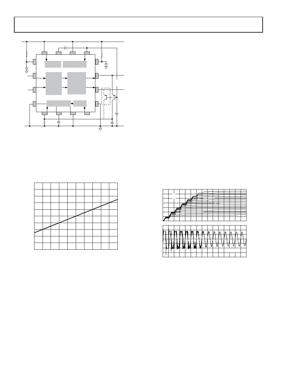
Figure 64. Simple AGC Amplifier (Preliminary)
When the loop is settled, the average current in Q1 is VDBS/R1,
which varies from 2 μA at maximum gain (VDBS = 0.2 V) to
17 μA at minimum gain (VDBS = 1.7 V). This change in the Q1
current causes an increase of ~0.25 dB over the full gain range
in the differential output of nominally 0.75 dBV at midrange
(3.08 V p-p), corresponding to a 200:1 compression ratio. This
is plotted in Figure 65 for a representative 100 kHz input.
INPUT TO AD8330 (dBV)
1.0
0
2
–
0
4
–
0
5
–
L
EVEL
ED
O
U
T
PU
T
(d
B
V)
0.8
0.7
0.6
0.5
–30
0.9
–10
03217-
066
Figure 65. AGC Output vs. Input Amplitude (Simulation)
The upper panel in Figure 66 shows the time-domain output for
fourteen 3 dB steps in input amplitude from 5.4 mV to 1.7 V.
This simple detector exhibits a temperature variation in the
differential output amplitude of about 4 mV/°C. It provides a
fast attack time (an increase in the input is quickly leveled to the
nominal output, due to the high peak currents in Q1) and a
slow release time (a decrease in the input is not restored as
quickly). The voltage at the VDBS pin can be used as an RSSI
output, scaled 30 mV/dB. Note that the attack time can be
halved by adding a second transistor, labeled Q2 in Figure 64.
For operation at lower frequencies, the AGC hold capacitor
must be increased.
WIDE RANGE TRUE RMS VOLTMETER
The AD8362 is an rms responding detector providing a
dynamic range of 60 dB from low frequencies to 2.7 GHz.
This can increase to 110 dB using an AD8330 as a precondi-
tioner, provided the noise bandwidth is limited by an interstage
low-pass or band-pass filter.
The VGA also provides an input port that is easier to drive
general scheme.
Both the AD8330 and AD8362 provide linear-in-decibel control
interfaces. Thus, when the output of the AD8362 is used to control
the gain of the AD8330, the functional form is unaffected. The
overall scaling is 33 mV/dB. Figure 68 shows the time domain
response using a loop filter capacitor of 10 nF, for inputs rang-
ing from 10 μV to 1 V rms, that is, a 100 dB measurement range.
TIME (s)
0
G
AI
N
E
R
O
R
(
d
B)
–1
1
–3
3
10
20
30
40
50
60
70
80
90
100 110 120 130 140 150
–2
0
–4
2
0.75
1.25
0.25
1.75
0.50
1.00
0
1.50
VDBS
OUTPUT
03217-
067
Figure 66. Time Domain Waveforms (Simulation)
相关PDF资料 |
PDF描述 |
|---|---|
| 3-1445055-1 | CONN HEADER 3MM 11POS R/A TIN |
| 2020-42T-ALF | GAS DISCHARGE TUBE 3 POLE 360V |
| 170M5265 | FUSE 900A 690V 2KN/110 AR UC |
| AD713JRZ-16-REEL | IC OPAMP BIFET QUAD PREC 16SOIC |
| 77313-118-40LF | BERGSTIK |
相关代理商/技术参数 |
参数描述 |
|---|---|
| AD8330-EVAL | 制造商:AD 制造商全称:Analog Devices 功能描述:Low Cost, DC to 150 MHz Variable Gain Amplifier |
| AD8330-EVALZ | 功能描述:BOARD EVAL FOR AD8330 RoHS:是 类别:编程器,开发系统 >> 评估板 - 运算放大器 系列:- 产品培训模块:Lead (SnPb) Finish for COTS Obsolescence Mitigation Program 标准包装:1 系列:- |
| AD8331 | 制造商:AD 制造商全称:Analog Devices 功能描述:Ultralow Noise VGAs with Preamplifier and Programmable RIN |
| AD8331_06 | 制造商:AD 制造商全称:Analog Devices 功能描述:Ultralow Noise VGAs with Preamplifier and Programmable RIN |
| AD8331_10 | 制造商:AD 制造商全称:Analog Devices 功能描述:Ultralow Noise VGAs with Preamplifier and Programmable RIN |
发布紧急采购,3分钟左右您将得到回复。