参数资料
| 型号: | AD8330ARQZ-RL |
| 厂商: | Analog Devices Inc |
| 文件页数: | 15/32页 |
| 文件大小: | 0K |
| 描述: | IC AMP VGA 150MHZ LN LP 16QSOP |
| 标准包装: | 2,500 |
| 放大器类型: | 可变增益 |
| 电路数: | 1 |
| 输出类型: | 差分,满摆幅 |
| 转换速率: | 1500 V/µs |
| -3db带宽: | 150MHz |
| 电流 - 输入偏压: | 100nA |
| 电流 - 电源: | 20mA |
| 电压 - 电源,单路/双路(±): | 2.7 V ~ 6 V |
| 工作温度: | -40°C ~ 85°C |
| 安装类型: | 表面贴装 |
| 封装/外壳: | 16-SSOP(0.154",3.90mm 宽) |
| 供应商设备封装: | 16-QSOP |
| 包装: | 带卷 (TR) |
| 配用: | AD8330-EVALZ-ND - BOARD EVAL FOR AD8330 |
第1页第2页第3页第4页第5页第6页第7页第8页第9页第10页第11页第12页第13页第14页当前第15页第16页第17页第18页第19页第20页第21页第22页第23页第24页第25页第26页第27页第28页第29页第30页第31页第32页
AD8330
Data Sheet
Rev. F | Page 22 of 32
FREQUENCY (Hz)
90
50k
CM
RR
(
d
B)
–10
10
30
50
70
M
0
1
M
1
k
0
1
80
0
20
40
60
10M
OFST: ENABLED
DISABLED
VDBS = 1.5V
VDBS = 0.75V
VDBS = 0V
03217-
060
Figure 59. Input CMRR vs. Frequency for Various Values of VDBS
FREQUENCY (Hz)
30
1M
–600
P
HAS
E
(
Deg
rees)
–20
–30
–10
0
10
20
–400
–300
–200
–100
0
LINE 1
LINE 3
LINE 4
LINE 2
LINE 4
LINE 1
LINE 3
LINE 2
10M
100M
500M
–500
03217-
061
G
AI
N
(
d
B)
Figure 60. AC Gain and Phase for Various Loading Conditions
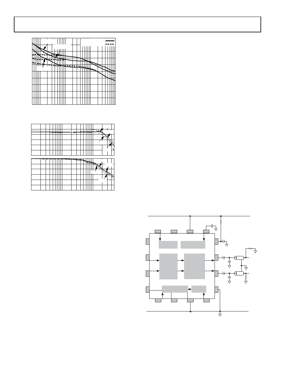
When driving a single-sided load, either OPHI or OPLO can be
used. These outputs are very symmetric, so the only effect of
this choice is to select the desired polarity. However, when the
frequency range of interest extends to the upper limits of the
AD8330, a dummy resistor of the same value should be attached
to the unused output. Figure 60 illustrates the ac gain and phase
response for various loads and VDBS = 0.75 V. Line 1 shows the
unloaded (CL = 12 pF) case for reference; the gain is 6 dB lower
(20 dB) using only the single-sided output. Adding a 75 Ω load
from OPHI to an ac ground results in Line 2. The gain becomes
a factor of ×1.5 V or 3.54 dB lower, but artifacts of the output
common-mode control loop appear in both the magnitude and
phase response.
Adding a dummy 75 Ω to OPLO results in Line 3: the gain is a
further 2.5 dB lower, at about 14 dB. The CM artifacts are no
longer present but a small amount of peaking occurs. If objec-
tionable, this can be eliminated by raising both of the capacitors
on the output pins to 25 pF, as shown in Line 4 of Figure 60.
The gain reduction incurred both by using only one output and
by the additional effect of loading can be overcome by taking
advantage of the VMAG feature, provided primarily for just such
circumstances. Thus, to restore the basic gain in the first case
(Line 1), a 1 V source should be applied to this pin; to restore the
gain in the second case, this voltage should be raised by a factor
of ×1.5 to 1.5 V. In Case 3 and Case 4, a further factor of ×1.33
is needed to make up the 2.5 dB loss, that is, VMAG should be
raised to 2 V. With the restoration of gain, the peak output
swing at the load is, likewise restored to ±2 V.
Pulse Operation
When using the AD8330 in applications where its transient
response is of greater interest and the outputs are conveyed to
their loads via coaxial cables, the added capacitances can slightly
differ in value, and can be placed either at the sending or load
end of the cables, or divided between these nodes. Figure 61
shows an illustrative example where dual, 1 meter, 75 Ω cables
are driven through dc-blocking capacitors and are independently
terminated at ground level.
Because of the considerable variation between applications,
only general recommendations can be made with regard to
minimizing pulse overshoot and droop. The former can be
optimized by adding small load capacitances, if necessary;
the latter requires the use of sufficiently large capacitors (C1).
input amplitude of 450 mV (the actual combination is not
important), a rise time of 2 ns, and VMAG raised to 2.0 V. In the
upper waveforms, the load capacitors are both zero, and a small
amount of overshoot is visible; with 40 pF, the response is cleaner.
A shunt capacitance of 20 pF from OPHI to OPLO has a similar
effect. Coupling capacitors for this demonstration are suffi-
ciently large to prevent any visible droop over this time scale.
The outputs at the load side eventually assume a mean value of
zero, with negative and positive excursions depending on the
duty cycle.
COMM
OPHI
INLO
OPLO
INHI
VPSI
VPSO
CMOP
MODE
VDBS
CMGN
VMAG
OFST
R
T
N
C
L
B
N
E
VPOS
BIAS AND
V-REF
GAIN INTERFACE
CM MODE AND
OFFSET CONTROL
OUTPUT
STAGES
OUTPUT
CONTROL
VGA CORE
NC
CD2
CD3
RD2
VS 2.7V–6V
C1
CL1
CL2
RL1
RL2
03217-
062
Figure 61. Driving Dual Cables with Grounded Loads
相关PDF资料 |
PDF描述 |
|---|---|
| 3-1445055-1 | CONN HEADER 3MM 11POS R/A TIN |
| 2020-42T-ALF | GAS DISCHARGE TUBE 3 POLE 360V |
| 170M5265 | FUSE 900A 690V 2KN/110 AR UC |
| AD713JRZ-16-REEL | IC OPAMP BIFET QUAD PREC 16SOIC |
| 77313-118-40LF | BERGSTIK |
相关代理商/技术参数 |
参数描述 |
|---|---|
| AD8330-EVAL | 制造商:AD 制造商全称:Analog Devices 功能描述:Low Cost, DC to 150 MHz Variable Gain Amplifier |
| AD8330-EVALZ | 功能描述:BOARD EVAL FOR AD8330 RoHS:是 类别:编程器,开发系统 >> 评估板 - 运算放大器 系列:- 产品培训模块:Lead (SnPb) Finish for COTS Obsolescence Mitigation Program 标准包装:1 系列:- |
| AD8331 | 制造商:AD 制造商全称:Analog Devices 功能描述:Ultralow Noise VGAs with Preamplifier and Programmable RIN |
| AD8331_06 | 制造商:AD 制造商全称:Analog Devices 功能描述:Ultralow Noise VGAs with Preamplifier and Programmable RIN |
| AD8331_10 | 制造商:AD 制造商全称:Analog Devices 功能描述:Ultralow Noise VGAs with Preamplifier and Programmable RIN |
发布紧急采购,3分钟左右您将得到回复。