参数资料
| 型号: | AD9042ASTZ |
| 厂商: | Analog Devices Inc |
| 文件页数: | 6/24页 |
| 文件大小: | 0K |
| 描述: | IC ADC 12BIT 41MSPS 44-TQFP |
| 标准包装: | 1 |
| 位数: | 12 |
| 采样率(每秒): | 41M |
| 数据接口: | 并联 |
| 转换器数目: | 3 |
| 功率耗散(最大): | 735mW |
| 电压电源: | 模拟和数字,双 ± |
| 工作温度: | -40°C ~ 85°C |
| 安装类型: | 表面贴装 |
| 封装/外壳: | 44-LQFP |
| 供应商设备封装: | 44-LQFP(10x10) |
| 包装: | 托盘 |
| 输入数目和类型: | 1 个单端,双极 |
| 产品目录页面: | 780 (CN2011-ZH PDF) |
AD9042
Rev. B | Page 14 of 24
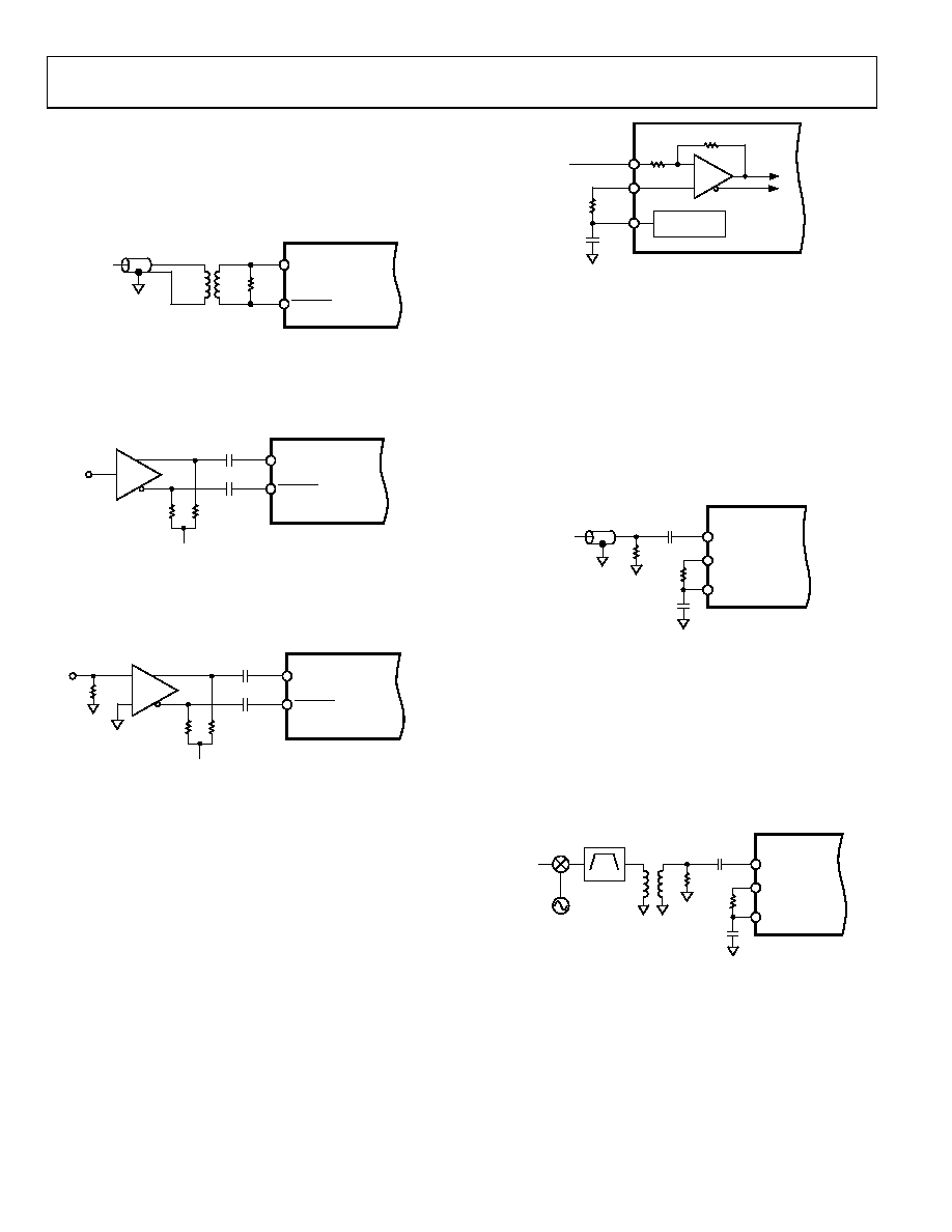
If no TTL source is available, a clean sine wave can be substituted.
In the case of the sine source, the matching network is shown in
Figure 29. Because the matching transformer specified is a 1:1
impedance ratio, R, the load resistor should be selected to
match the source impedance. The input impedance of the
AD9042 is negligible in most cases.
ENCODE
AD9042
R
T1-1T
SINE
SOURCE
ENCODE
0
55
4-
0
35
Figure 29. Sine Source Differential Encode
If a low jitter ECL clock is available, another option is to ac-
couple a differential ECL signal to the encode input pins as
shown in Figure 30. The capacitors shown here should be chip
capacitors but do not need to be of the low inductance variety.
ENCODE
AD9042
ECL
GATE
0.1F
510
510
–VS
ENCODE
00
55
4-
0
36
Figure 30. Differential ECL for Encode
As a final alternative, the ECL gate can be replaced by an ECL
comparator. The input to the comparator could then be a logic
signal or a sine signal.
ENCODE
AD9042
AD96687 (1/2)
0.1F
510
510
50
–VS
ENCODE
+
–
00
55
4-
0
37
Figure 31. ECL Comparator for Encode
Care should be taken not to overdrive the encode input pins
when ac-coupled. Although the input circuitry is electrically
protected from overvoltage or undervoltage conditions,
improper circuit operations may result from overdriving the
encode input pins.
DRIVING THE ANALOG INPUT
Because the AD9042 operates from a single 5 V supply, the
analog input range is offset from ground by 2.4 V. The analog input,
AIN, is an operational amplifier configured in an inverting mode
Because the operational amplifier forces its inputs to the same
voltage, the inverting input is also at 2.4 V. Therefore, the analog
input has a Thevenin equivalent of 250 Ω in series with a 2.4 V
source. It is strongly recommended that the internal voltage
reference of the AD9042 be used for the amplifier offset; this
reference is designed to track internal circuit shifts over
temperature.
AD9042
2.4V
REFERENCE
AIN
0.1F
VOFFSET
TIED TO
VREF
THROUGH
50
250
250
50
+
–
00
55
4-
0
38
Figure 32. Analog Input Offset by 2.4 V Reference
Although the AD9042 can be used in many applications, it was
specifically designed for communications systems that must
digitize wide signal bandwidths. As such, the analog input was
designed to be ac-coupled. Because most communications
products do not downconvert to dc, this should not pose a
problem. One example of a typical analog input circuit is shown
in Figure 33. In this application, the analog input is coupled
with a high quality chip capacitor, the value of which can be
chosen to provide a low frequency cutoff that is consistent with
the signal being sampled; in most cases, a 0.1 μF chip capacitor
works well.
0.1F
AIN
AD9042
VOFFSET
VREF
ANALOG
SIGNAL
SOURCE
RT
50
00
55
4-
0
39
Figure 33. AC-Coupled Analog Input Signal
Another option for ac coupling is a transformer. The impedance
ratio and frequency characteristics of the transformer are
determined by examining the characteristics of the input signal
source (transformer primary connection), and the AD9042
input characteristics (transformer secondary connection).
Given the transformer turns ratio, RT should be chosen to
satisfy the termination requirements of the source. A blocking
capacitor is required to prevent AD9042 dc bias currents from
flowing through the transformer.
0.1F
AIN
AD9042
VOFFSET
VREF
ANALOG
SIGNAL
SOURCE
RT
50
XFMR
LO
BPF
00
55
4-
0
40
Figure 34. Transformer-Coupled Analog Input Signal
相关PDF资料 |
PDF描述 |
|---|---|
| AD9051BRSRL-2V | IC ADC 10BIT 60MSPS 28-SSOP |
| AD9054ABSTZ-200 | IC ADC 8BIT 200MSPS 44-LQFP |
| AD9057BRS-RL40 | IC ADC 8BIT 40MSPS 20-SSOP T/R |
| AD9058AKD | IC ADC 8BIT DUAL 50MSPS 48-CDIP |
| AD9059BRS | IC ADC 8BIT DUAL 60MSPS 28-SSOP |
相关代理商/技术参数 |
参数描述 |
|---|---|
| AD9042BD | 制造商:Analog Devices 功能描述:- Bulk |
| AD9042CHIPS | 制造商:AD 制造商全称:Analog Devices 功能描述:12-Bit, 41 MSPS Monolithic A/D Converter |
| AD9042D | 制造商:AD 制造商全称:Analog Devices 功能描述:12-Bit, 41 MSPS Monolithic A/D Converter |
| AD9042D/PCB | 制造商:AD 制造商全称:Analog Devices 功能描述:12-Bit, 41 MSPS Monolithic A/D Converter |
| AD9042DPCB | 制造商:AD 制造商全称:Analog Devices 功能描述:12-Bit, 41 MSPS Monolithic A/D Converter |
发布紧急采购,3分钟左右您将得到回复。