- 您现在的位置:买卖IC网 > PDF目录8657 > AD9114BCPZRL7 (Analog Devices Inc)IC DAC DUAL 8BIT LO PWR 40LFCSP PDF资料下载
参数资料
| 型号: | AD9114BCPZRL7 |
| 厂商: | Analog Devices Inc |
| 文件页数: | 2/52页 |
| 文件大小: | 0K |
| 描述: | IC DAC DUAL 8BIT LO PWR 40LFCSP |
| 产品培训模块: | Data Converter Fundamentals DAC Architectures |
| 标准包装: | 750 |
| 系列: | TxDAC® |
| 位数: | 8 |
| 数据接口: | 串行 |
| 转换器数目: | 2 |
| 电压电源: | 模拟和数字 |
| 功率耗散(最大): | 232mW |
| 工作温度: | -40°C ~ 85°C |
| 安装类型: | 表面贴装 |
| 封装/外壳: | 40-VFQFN 裸露焊盘,CSP |
| 供应商设备封装: | 40-LFCSP-VQ(6x6) |
| 包装: | 带卷 (TR) |
| 输出数目和类型: | 4 电流,单极 |
| 采样率(每秒): | 125M |
第1页当前第2页第3页第4页第5页第6页第7页第8页第9页第10页第11页第12页第13页第14页第15页第16页第17页第18页第19页第20页第21页第22页第23页第24页第25页第26页第27页第28页第29页第30页第31页第32页第33页第34页第35页第36页第37页第38页第39页第40页第41页第42页第43页第44页第45页第46页第47页第48页第49页第50页第51页第52页
AD9114/AD9115/AD9116/AD9117
Data Sheet
Rev. C | Page 10 of 52
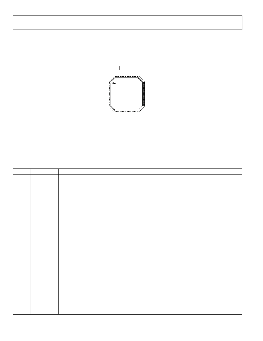
PIN CONFIGURATIONS AND FUNCTION DESCRIPTIONS
PIN 1
INDICATOR
1
DB5
2
DB4
3
DB3
4
DB2
5
DVDDIO
6
DVSS
7
DVDD
8
DB1
9
DB0 (LSB)
10
NC
23
24
25
26
27
28
29
30
22
21
1
NC
12
NC
13
NC
15
NC
17
CV
DD
16
DCL
KI
O
18
CL
KI
N
19
C
VSS
20
CM
L
Q
14
NC
33
F
S
ADJI
/AUX
I
34
R
E
FIO
35
R
ESET
/PI
N
MD
36
S
CL
K/
CL
KM
D
37
S
D
IO/FOR
M
A
T
38
CS
/P
W
RDN
39
DB7
(
M
S
B)
40
DB6
32
F
S
ADJQ
/AUX
Q
31
CM
L
I
TOP VIEW
(Not to Scale)
AD9114
07466-
005
NOTES
1. NC = NO CONNECT
2. THE EXPOSED PAD IS CONNECTED TO AVSS AND
MUST BE SOLDERED TO THE GROUND PLANE.
EXPOSED METAL AT PACKAGE CORNERS IS
CONNECTED TO THIS PAD.
QOUTP
RLQP
AVSS
AVDD
RLIP
IOUTP
IOUTN
RLIN
QOUTN
RLQN
Figure 2. AD9114 Pin Configuration
Table 7. AD9114 Pin Function Descriptions
Pin No.
Mnemonic
Description
1 to 4
DB[5:2]
Digital Inputs.
5
DVDDIO
Digital I/O Supply Voltage Input (1.8 V to 3.3 V Nominal).
6
DVSS
Digital Common.
7
DVDD
Digital Core Supply Voltage Output (1.8 V). Strap DVDD to DVDDIO at 1.8 V. If DVDDIO > 1.8 V, bypass DVDD
with a 1.0 F capacitor; however, do not otherwise connect it. The LDO should not drive external loads.
8
DB1
Digital Inputs
9
DB0 (LSB)
Digital Input (LSB).
10 to
15
NC
No Connect. These pins are not connected to the chip.
16
DCLKIO
Data Input/Output Clock. Clock used to qualify input data.
17
CVDD
Sampling Clock Supply Voltage Input (1.8 V to 3.3 V). CVDD must be ≥ DVDD.
18
CLKIN
LVCMOS Sampling Clock Input.
19
CVSS
Sampling Clock Supply Voltage Common.
20
CMLQ
Q DAC Output Common-Mode Level. When the internal on-chip (QRCML) is enabled, this pin is connected to
the on-chip QRCML resistor. It is recommended to leave this pin unconnected. When the internal on-chip (QRCML) is
disabled, this pin is the common-mode load for Q DAC and must be connected to AVSS through a resistor, see
the Using the Internal Termination Resistors section. Recommended value for this external resistor is 0 .
21
RLQN
Load Resistor (62.5 ) to the CMLQ Pin. For the internal load resistor to be used, this pin should be tied to
QOUTN externally.
22
QOUTN
Complementary Q DAC Current Output. Full-scale current is sourced when all data bits are 0s.
23
QOUTP
Q DAC Current Output. Full-scale current is sourced when all data bits are 1s.
24
RLQP
Load Resistor (62.5 ) to the CMLQ Pin. For the internal load resistor to be used, this pin should be tied to
QOUTP externally.
25
AVSS
Analog Common.
26
AVDD
Analog Supply Voltage Input (1.8 V to 3.3 V).
27
RLIP
Load Resistor (62.5 ) to the CMLI Pin. For the internal load resistor to be used, this pin should be tied to
IOUTP externally.
28
IOUTP
I DAC Current Output. Full-scale current is sourced when all data bits are 1s.
相关PDF资料 |
PDF描述 |
|---|---|
| IDT49FCT3805QI | IC CLK BUFFER 1:5 100MHZ 20-QSOP |
| V110A15H400BG2 | CONVERTER MOD DC/DC 15V 400W |
| VI-J6Y-MY | CONVERTER MOD DC/DC 3.3V 33W |
| VI-J0H-MX-B1 | CONVERTER MOD DC/DC 52V 75W |
| VI-J6Y-MX | CONVERTER MOD DC/DC 3.3V 49.5W |
相关代理商/技术参数 |
参数描述 |
|---|---|
| AD9114-DPG2-EBZ | 功能描述:IC DAC DUAL 8BIT LO PWR 40LFCSP RoHS:是 类别:编程器,开发系统 >> 评估板 - 数模转换器 (DAC) 系列:TxDAC® 产品培训模块:Lead (SnPb) Finish for COTS Obsolescence Mitigation Program 标准包装:1 系列:- DAC 的数量:4 位数:12 采样率(每秒):- 数据接口:串行,SPI? 设置时间:3µs DAC 型:电流/电压 工作温度:-40°C ~ 85°C 已供物品:板 已用 IC / 零件:MAX5581 |
| AD9114-EBZ | 制造商:Analog Devices 功能描述:DUAL 8 BIT LOW POWER CONVERTER - Boxed Product (Development Kits) |
| AD9115 | 制造商:AD 制造商全称:Analog Devices 功能描述:Dual, 8-/10-/12-/14-Bit Low Power Digital-to-Analog Converters |
| AD91151Z | 制造商:Analog Devices 功能描述: |
| AD91154Z | 制造商:Analog Devices 功能描述:SCREENED DSP PART - Rail/Tube |
发布紧急采购,3分钟左右您将得到回复。