- 您现在的位置:买卖IC网 > PDF目录8657 > AD9114BCPZRL7 (Analog Devices Inc)IC DAC DUAL 8BIT LO PWR 40LFCSP PDF资料下载
参数资料
| 型号: | AD9114BCPZRL7 |
| 厂商: | Analog Devices Inc |
| 文件页数: | 28/52页 |
| 文件大小: | 0K |
| 描述: | IC DAC DUAL 8BIT LO PWR 40LFCSP |
| 产品培训模块: | Data Converter Fundamentals DAC Architectures |
| 标准包装: | 750 |
| 系列: | TxDAC® |
| 位数: | 8 |
| 数据接口: | 串行 |
| 转换器数目: | 2 |
| 电压电源: | 模拟和数字 |
| 功率耗散(最大): | 232mW |
| 工作温度: | -40°C ~ 85°C |
| 安装类型: | 表面贴装 |
| 封装/外壳: | 40-VFQFN 裸露焊盘,CSP |
| 供应商设备封装: | 40-LFCSP-VQ(6x6) |
| 包装: | 带卷 (TR) |
| 输出数目和类型: | 4 电流,单极 |
| 采样率(每秒): | 125M |
第1页第2页第3页第4页第5页第6页第7页第8页第9页第10页第11页第12页第13页第14页第15页第16页第17页第18页第19页第20页第21页第22页第23页第24页第25页第26页第27页当前第28页第29页第30页第31页第32页第33页第34页第35页第36页第37页第38页第39页第40页第41页第42页第43页第44页第45页第46页第47页第48页第49页第50页第51页第52页
AD9114/AD9115/AD9116/AD9117
Data Sheet
Rev. C | Page 34 of 52
MSB/LSB TRANSFERS
The serial port of the AD9114/AD9115/AD9116/AD9117 can
support both most significant bit (MSB) first or least significant
bit (LSB) first data formats. This functionality is controlled by the
LSBFIRST bit (Register 0x00, Bit 6). The default is MSB first
(LSBFIRST = 0).
When LSBFIRST = 0 (MSB first), the instruction and data bytes
must be written from the most significant bit to the least significant
bit. Multibyte data transfers in MSB first format start with an
instruction byte that includes the register address of the most
significant data byte. Subsequent data bytes should follow in
order from a high address to a low address. In MSB first mode,
the serial port internal byte address generator decrements for
each data byte of the multibyte communications cycle.
When LSBFIRST = 1 (LSB first), the instruction and data bytes
must be written from the least significant bit to the most significant
bit. Multibyte data transfers in LSB first format start with an
instruction byte that includes the register address of the least
significant data byte followed by multiple data bytes. The serial
port internal byte address generator increments for each byte of
the multibyte communication cycle.
If the MSB first mode is active, the serial port controller data
address of the AD9114/AD9115/AD9116/AD9117 decrements
from the data address written toward 0x00 for multibyte I/O
operations. If the LSB first mode is active, the serial port controller
address increments from the data address written toward 0x1F
for multibyte I/O operations.
SERIAL PORT OPERATION
The serial port configuration of the AD9114/AD9115/AD9116/
AD9117 is controlled by Register 0x00. It is important to note
that the configuration changes immediately upon writing to the
last bit of the register. For multibyte transfers, writing to this
register can occur during the middle of the communications
cycle. Care must be taken to compensate for this new configu-
ration for the remaining bytes of the current communications cycle.
The same considerations apply to setting the software reset bit
(Register 0x00, Bit 5). All registers are set to their default values
except Register 0x00, which remains unchanged.
Use of single-byte transfers or initiating a software reset is
recommended when changing serial port configurations to
prevent unexpected device behavior.
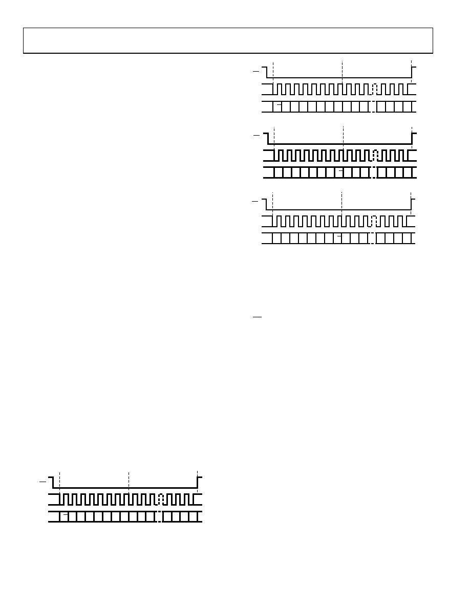
R/W N1N0A4 A3 A2 A1 A0 D7N D6N D5N
D00
D10
D20
D30
INSTRUCTION CYCLE
DATA TRANSFER CYCLE
CS
SCLK
SDIO
07
46
6-
29
1
Figure 85. Serial Register Interface Timing, MSB First Write
R/W N1N0A4A3 A2 A1 A0 D7N D6N D5N
D00
D10
D20
D30
INSTRUCTION CYCLE
DATA TRANSFER CYCLE
CS
SCLK
SDIO
07
466
-386
Figure 86. Serial Register Interface Timing, MSB First Read
A0 A1 A2 A3 A4 N0 N1 R/W D00 D10 D20
D7N
D6N
D5N
D4N
INSTRUCTION CYCLE
DATA TRANSFER CYCLE
SCLK
SDIO
0
74
66
-289
CS
Figure 87. Serial Register Interface Timing, LSB First Write
A0 A1 A2 A3 A4 N0 N1 R/W D00 D10 D20
D7N
D6N
D5N
D4N
INSTRUCTION CYCLE
DATA TRANSFER CYCLE
SCLK
SDIO
CS
07
46
6-
38
8
Figure 88. Serial Register Interface Timing, LSB First Read
PIN MODE
The AD9114/AD9115/AD9116/AD9117 can also be operated
without ever writing to the serial port. With RESET/PINMD
(Pin 35) tied high, the SCLK pin becomes CLKMD to provide
for clock mode control (see the Retimer section), the SDIO
pin becomes FORMAT and selects the input data format, and
the CS/PWRDN pin serves to power down the device. The
pins are not latched at power up. If you change the format, it
should change with about a 1μs delay.
Operation is otherwise exactly as defined by the default register
values in Table 13; therefore, external resistors at FSADJI and
FSADJQ are needed to set the DAC currents, and both DACs
are active. This is also a convenient quick checkout mode. DAC
currents can be externally adjusted in pin mode by sourcing or
sinking currents at the FSADJI/AUXI and FSADJQ/AUXQ
pins, as desired, with the fixed resistors installed. An op amp
output with appropriate series resistance is one of many
possibilities. This has the same effect as changing the resistor
value. Place at least 10 kΩ resistors in series right at the DAC
to guard against accidental short circuits and noise
modulation. The REFIO pin can be adjusted ±25% in a similar
manner, if desired.
相关PDF资料 |
PDF描述 |
|---|---|
| IDT49FCT3805QI | IC CLK BUFFER 1:5 100MHZ 20-QSOP |
| V110A15H400BG2 | CONVERTER MOD DC/DC 15V 400W |
| VI-J6Y-MY | CONVERTER MOD DC/DC 3.3V 33W |
| VI-J0H-MX-B1 | CONVERTER MOD DC/DC 52V 75W |
| VI-J6Y-MX | CONVERTER MOD DC/DC 3.3V 49.5W |
相关代理商/技术参数 |
参数描述 |
|---|---|
| AD9114-DPG2-EBZ | 功能描述:IC DAC DUAL 8BIT LO PWR 40LFCSP RoHS:是 类别:编程器,开发系统 >> 评估板 - 数模转换器 (DAC) 系列:TxDAC® 产品培训模块:Lead (SnPb) Finish for COTS Obsolescence Mitigation Program 标准包装:1 系列:- DAC 的数量:4 位数:12 采样率(每秒):- 数据接口:串行,SPI? 设置时间:3µs DAC 型:电流/电压 工作温度:-40°C ~ 85°C 已供物品:板 已用 IC / 零件:MAX5581 |
| AD9114-EBZ | 制造商:Analog Devices 功能描述:DUAL 8 BIT LOW POWER CONVERTER - Boxed Product (Development Kits) |
| AD9115 | 制造商:AD 制造商全称:Analog Devices 功能描述:Dual, 8-/10-/12-/14-Bit Low Power Digital-to-Analog Converters |
| AD91151Z | 制造商:Analog Devices 功能描述: |
| AD91154Z | 制造商:Analog Devices 功能描述:SCREENED DSP PART - Rail/Tube |
发布紧急采购,3分钟左右您将得到回复。