- 您现在的位置:买卖IC网 > PDF目录17100 > AD9146-M5375-EBZ (Analog Devices Inc)BOARD EVAL FOR AD9146 DAC PDF资料下载
参数资料
| 型号: | AD9146-M5375-EBZ |
| 厂商: | Analog Devices Inc |
| 文件页数: | 31/56页 |
| 文件大小: | 0K |
| 描述: | BOARD EVAL FOR AD9146 DAC |
| 设计资源: | AD9146-M5375-EBZ Schematic AD9146-M5375-EBZ Gerber Files |
| 标准包装: | 1 |
| 系列: | TxDAC+® |
| DAC 的数量: | 2 |
| 位数: | 16 |
| 采样率(每秒): | 1G |
| 数据接口: | 串行 |
| 设置时间: | 20ns |
| DAC 型: | 电流 |
| 工作温度: | -40°C ~ 85°C |
| 已供物品: | 板 |
| 已用 IC / 零件: | AD9146 |
第1页第2页第3页第4页第5页第6页第7页第8页第9页第10页第11页第12页第13页第14页第15页第16页第17页第18页第19页第20页第21页第22页第23页第24页第25页第26页第27页第28页第29页第30页当前第31页第32页第33页第34页第35页第36页第37页第38页第39页第40页第41页第42页第43页第44页第45页第46页第47页第48页第49页第50页第51页第52页第53页第54页第55页第56页
Data Sheet
AD9146
Rev. A | Page 37 of 56
DAC INPUT CLOCK CONFIGURATIONS
The AD9146 DAC sampling clock (DACCLK) can be sourced
directly or by clock multiplying. Clock multiplying uses the
on-chip phase-locked loop (PLL), which accepts a reference clock
operating at a submultiple of the desired DACCLK rate, most
commonly the data input frequency. The PLL then multiplies
the reference clock up to the desired DACCLK frequency, which
can then be used to generate all the internal clocks required by
the DAC. The clock multiplier provides a high quality clock that
meets the performance requirements of most applications. Using
the on-chip clock multiplier eliminates the need to generate and
distribute the high speed DACCLK.
The second mode bypasses the clock multiplier circuitry and
allows the DACCLK to be sourced directly to the DAC core.
This mode enables the user to source a very high quality clock
directly to the DAC core. Sourcing the DACCLK directly through
the REFCLKP, REFCLKN, DACCLKP, and DACCLKN pins may
be necessary in demanding applications that require the lowest
possible DAC output noise, particularly when directly synthesizing
signals above 150 MHz.
DRIVING THE DACCLK AND REFCLK INPUTS
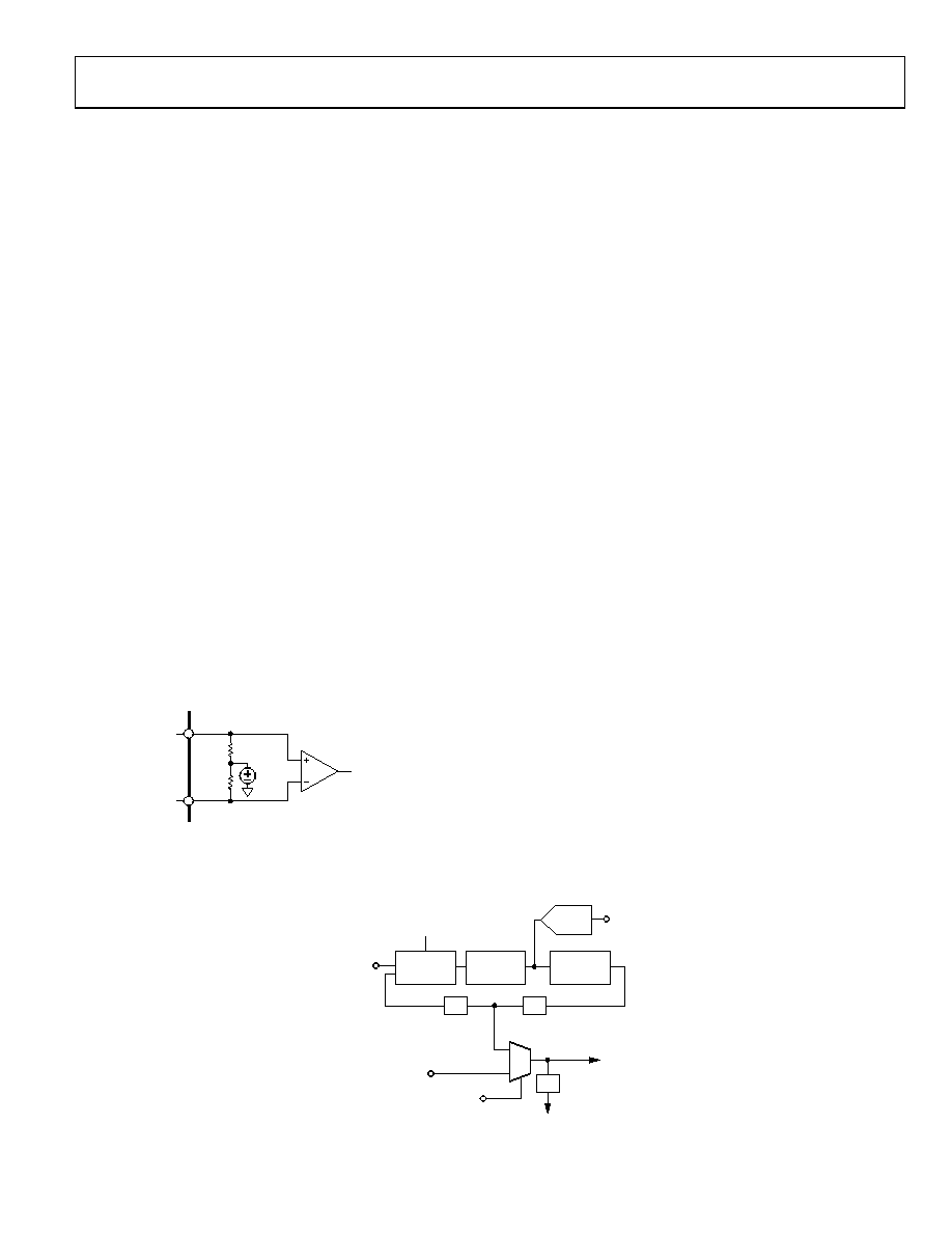
The differential DACCLK and REFCLK inputs share similar
clock receiver input circuitry. Figure 47 shows a simplified circuit
diagram of the inputs. The on-chip clock receiver has a differential
input impedance of about 10 k. It is self-biased to a common-
mode voltage of about 1.25 V. The inputs can be driven by
direct coupling differential PECL or LVDS drivers. The inputs
can also be ac-coupled if the driving source cannot meet the
input compliance voltage of the receiver.
1.25V
5k
DACCLKP,
REFCLKP
DACCLKN,
REFCLKN
09691-
052
Figure 47. Clock Receiver Input Simplified Equivalent Circuit
The minimum input drive level to either of the clock inputs is
100 mV p-p differential. The optimal performance is achieved
when the clock input signal is between 800 mV p-p differential
and 1.6 V p-p differential. Whether using the on-chip clock
multiplier or sourcing the DACCLK directly, it is necessary that
the input clock signal to the device have low jitter and fast edge
rates to optimize the DAC noise performance.
DIRECT CLOCKING
Direct clocking with a low noise clock produces the lowest noise
spectral density at the DAC outputs. To select the differential
CLK inputs as the source for the DAC sampling clock, set the
PLL enable bit (Register 0x0A, Bit 7) to 0. This powers down
the internal PLL clock multiplier and selects the input from the
DACCLKP and DACCLKN pins as the source for the internal
DAC sampling clock.
The device also has duty cycle correction circuitry and differ-
ential input level correction circuitry. Enabling these circuits can
provide improved performance in some cases. The control bits
for these functions are in Register 0x08 (see Table 11).
CLOCK MULTIPLICATION
The on-chip PLL clock multiplication circuit can be used to gen-
erate the DAC sampling clock from a lower frequency reference
clock. When the PLL enable bit (Register 0x0A, Bit 7) is set to 1,
the clock multiplication circuit generates the DAC sampling clock
from the lower rate REFCLK input. The functional diagram of
the clock multiplier is shown in Figure 48.
The clock multiplication circuit operates such that the VCO
outputs a frequency, fVCO, equal to the REFCLK input signal
frequency multiplied by N1 × N0.
fVCO = fREFCLK × (N1 × N0)
The DAC sampling clock frequency, fDACCLK, is equal to
fDACCLK = fREFCLK × N1
The output frequency of the VCO must be chosen to keep fVCO
in the optimal operating range of 1.0 GHz to 2.1 GHz. The
frequency of the reference clock and the values of N1 and N0
must be chosen so that the desired DACCLK frequency can be
synthesized and the VCO output frequency is in the correct range.
DACCLKP/DACCLKN
(PIN 3 AND PIN 4)
ADC
VCO
LOOP
FILTER
REFCLKP/REFCLKN
(PIN 6 AND PIN 7)
REG 0x0E[3:0]
VCO CONTROL
VOLTAGE
REG 0x0D[3:2]
N0
REG 0x0D[1:0]
N1
÷N1
÷N0
REG 0x06[7:6]
PLL LOCK LOST
PLL LOCKED
PHASE
DETECTION
REG 0x0A[7]
PLL ENABLE
REG 0x0D[7:6]
N2
÷N2
DACCLK
PC_CLK
09691-
053
Figure 48. PLL Clock Multiplication Circuit
相关PDF资料 |
PDF描述 |
|---|---|
| MCP355XDM-TAS | BOARD DEMO TINY APP SNSR MCP355X |
| LGU2D271MELY | CAP ALUM 270UF 200V 20% SNAP |
| MCP3551DM-PCTL | BOARD DEMO FOR MCP3551 |
| 0210490181 | CABLE JUMPER 1.25MM .203M 12POS |
| HL02150GTTR | INDUCTOR 15NH 200MA 0402 |
相关代理商/技术参数 |
参数描述 |
|---|---|
| AD9148 | 制造商:AD 制造商全称:Analog Devices 功能描述:Quad 16-Bit,1 GSPS, TxDAC+ Digital-to-Analog Converter |
| AD9148ARUZ | 制造商:Analog Devices 功能描述:- Rail/Tube |
| AD9148BBCZ | 功能描述:IC DAC 16BIT QD 1GSPS 196CSPBGA RoHS:是 类别:集成电路 (IC) >> 数据采集 - 数模转换器 系列:TxDAC+® 标准包装:1 系列:- 设置时间:4.5µs 位数:12 数据接口:串行,SPI? 转换器数目:1 电压电源:单电源 功率耗散(最大):- 工作温度:-40°C ~ 125°C 安装类型:表面贴装 封装/外壳:8-SOIC(0.154",3.90mm 宽) 供应商设备封装:8-SOICN 包装:剪切带 (CT) 输出数目和类型:1 电压,单极;1 电压,双极 采样率(每秒):* 其它名称:MCP4921T-E/SNCTMCP4921T-E/SNRCTMCP4921T-E/SNRCT-ND |
| AD9148BBCZRL | 功能描述:IC DAC 16BIT QD 1GSPS 196CSPBGA RoHS:否 类别:集成电路 (IC) >> 数据采集 - 数模转换器 系列:TxDAC+® 产品培训模块:Lead (SnPb) Finish for COTS Obsolescence Mitigation Program 标准包装:1,000 系列:- 设置时间:1µs 位数:8 数据接口:串行 转换器数目:8 电压电源:双 ± 功率耗散(最大):941mW 工作温度:0°C ~ 70°C 安装类型:表面贴装 封装/外壳:24-SOIC(0.295",7.50mm 宽) 供应商设备封装:24-SOIC W 包装:带卷 (TR) 输出数目和类型:8 电压,单极 采样率(每秒):* |
| AD9148BBPZ | 功能描述:IC DAC 16BIT SPI/SRL 196BGA RoHS:是 类别:集成电路 (IC) >> 数据采集 - 数模转换器 系列:TxDAC+® 标准包装:1 系列:- 设置时间:4.5µs 位数:12 数据接口:串行,SPI? 转换器数目:1 电压电源:单电源 功率耗散(最大):- 工作温度:-40°C ~ 125°C 安装类型:表面贴装 封装/外壳:8-SOIC(0.154",3.90mm 宽) 供应商设备封装:8-SOICN 包装:剪切带 (CT) 输出数目和类型:1 电压,单极;1 电压,双极 采样率(每秒):* 其它名称:MCP4921T-E/SNCTMCP4921T-E/SNRCTMCP4921T-E/SNRCT-ND |
发布紧急采购,3分钟左右您将得到回复。