- 您现在的位置:买卖IC网 > PDF目录17100 > AD9146-M5375-EBZ (Analog Devices Inc)BOARD EVAL FOR AD9146 DAC PDF资料下载
参数资料
| 型号: | AD9146-M5375-EBZ |
| 厂商: | Analog Devices Inc |
| 文件页数: | 43/56页 |
| 文件大小: | 0K |
| 描述: | BOARD EVAL FOR AD9146 DAC |
| 设计资源: | AD9146-M5375-EBZ Schematic AD9146-M5375-EBZ Gerber Files |
| 标准包装: | 1 |
| 系列: | TxDAC+® |
| DAC 的数量: | 2 |
| 位数: | 16 |
| 采样率(每秒): | 1G |
| 数据接口: | 串行 |
| 设置时间: | 20ns |
| DAC 型: | 电流 |
| 工作温度: | -40°C ~ 85°C |
| 已供物品: | 板 |
| 已用 IC / 零件: | AD9146 |
第1页第2页第3页第4页第5页第6页第7页第8页第9页第10页第11页第12页第13页第14页第15页第16页第17页第18页第19页第20页第21页第22页第23页第24页第25页第26页第27页第28页第29页第30页第31页第32页第33页第34页第35页第36页第37页第38页第39页第40页第41页第42页当前第43页第44页第45页第46页第47页第48页第49页第50页第51页第52页第53页第54页第55页第56页
AD9146
Data Sheet
Rev. A | Page 48 of 56
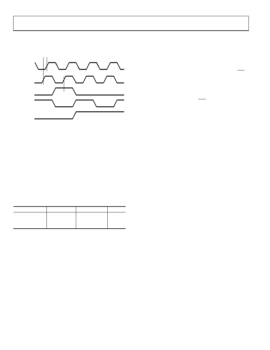
When these conditions are met, the outputs of the DACs are
updated within one DAC clock cycle of each other. The timing
requirements of the input signals are shown in Figure 67.
DACCLKP(1)/
DACCLKN(1)
DACCLKP(2)/
DACCLKN(2)
REFCLKP(2)/
REFCLKN(2)
DCIP(2)/
DCIN(2)
FRAMEP(2)/
FRAMEN(2)
tSKEW
tSUSYNC
tHSYNC
09691-
073
Figure 67. FIFO Rate Synchronization Signal Timing Requirements,
2× Interpolation
Figure 67 shows the synchronization signal timing with 2×
interpolation; therefore, fDCI = × fCLK. The REFCLK input is
shown to be equal to the FIFO rate. The maximum frequency at
which the device can be resynchronized in FIFO rate mode can
be expressed as
fSYNC_I = fDATA/(8 × 2N)
where N is any non-negative integer.
ADDITIONAL SYNCHRONIZATION FEATURES
Table 25 shows the required timing between the DACCLK and the
synchronization clock when synchronization is used. This timing
restriction applies to both data rate mode and FIFO rate mode.
Table 25. Synchronization Setup and Hold Times
Parameter
Min
Max
Unit
tSKEW
tDACCLK/2
+tDACCLK/2
ps
tSUSYNC
100
ps
tHSYNC
330
ps
One-Time Synchronization
When implementing the full multichip synchronization feature
(with the REFCLK and FRAME signals aligned within one DACCLK
cycle), the user may experience difficulty meeting the DACCLK to
synchronization clock timing. In this case, a one-time synchroni-
zation method can be used. Before implementing the one-time
synchronization, make sure that the synchronization signal is
locked by checking both the sync signal locked and the sync signal
lost flags (Bit 4 and Bit 5 in Register 0x06). It is also important
that synchronization not be enabled before stable REFCLK signals
are present from the FPGA or ASIC. For more information and
a detailed flowchart of the one-time synchronization feature, see
the AN-1093 Application Note, “Synchronization of Multiple
AD9122 TxDAC+ Converters.”
Sync Status Bits
When the sync locked bit (Register 0x12, Bit 6) is set, it indicates
that the synchronization logic has reached alignment. This align-
ment is determined when the clock generation state machine
phase is constant.
Alignment takes from (11 + averaging) × 64 to (11 + averaging) ×
128 DACCLK cycles. The sync locked bit can also trigger an IRQ,
as described in the Interrupt Request Operation section.
When the sync lost bit (Register 0x12, Bit 7) is set, it indicates
that a previously synchronized device has lost alignment. This
bit is latched and remains set until cleared by overwriting the
register. This bit can also trigger an IRQ, as described in the
Interrupt Request Operation section.
The sync phase readback bits (Register 0x13, Bits[7:0]) report
the current clock phase in a 6.2 format. Bits[7:2] report which
of the 64 states (0 to 63) the clock is currently in. When averaging
is enabled, Bits[1:0] provide state accuracy (for 0, , , ).
The lower two bits give an indication of the timing margin issues
that may exist. If the synchronization sampling is error free, the
fractional clock state should be 00.
Timing Optimization
The REFCLK signal is sampled by a version of the DACCLK.
If sampling errors are detected, the opposite sampling edge can
be selected to improve the sampling point. The sampling edge
can be selected by setting Register 0x10, Bit 3 (1 = rising and
0 = falling).
The synchronization logic resynchronizes when a phase change
between the REFCLK signal and the state of the clock generation
state machine exceeds a threshold. To mitigate the effects of
jitter and prevent erroneous resynchronizations, the relative
phase can be averaged. The amount of averaging is set by the
sync averaging bits (Register 0x10, Bits[2:0]) and can be set
from 1 to 128. The higher the number of averages, the more
slowly the device recognizes and resynchronizes to a legitimate
phase correction. Generally, the averaging should be made as large
as possible while still meeting the allotted resynchronization
time interval. Note that, if the average synchronization sampling
result is in approximately the middle of the probability curve,
the synchronization engine can be unstable, resulting in
corrupted output.
The value of the Sync Phase Request[5:0] bits (Register 0x11,
Bits[5:0]) is the state to which the clock generation state machine
resets upon initialization. By varying this value, the timing of the
internal clocks, with respect to the REFCLK signal, can be adjusted.
Every increment of the Sync Phase Request[5:0] value advances the
internal clocks by one DACCLK cycle. This offset can be used for
two purposes: to skew the outputs of two synchronized DAC
outputs in increments of the DACCLK cycle, and to change the
relative timing between the DAC output and the sync input
(REFCLK). This may allow for a more optimal placement of the
DCI sampling point in data rate synchronization mode.
相关PDF资料 |
PDF描述 |
|---|---|
| MCP355XDM-TAS | BOARD DEMO TINY APP SNSR MCP355X |
| LGU2D271MELY | CAP ALUM 270UF 200V 20% SNAP |
| MCP3551DM-PCTL | BOARD DEMO FOR MCP3551 |
| 0210490181 | CABLE JUMPER 1.25MM .203M 12POS |
| HL02150GTTR | INDUCTOR 15NH 200MA 0402 |
相关代理商/技术参数 |
参数描述 |
|---|---|
| AD9148 | 制造商:AD 制造商全称:Analog Devices 功能描述:Quad 16-Bit,1 GSPS, TxDAC+ Digital-to-Analog Converter |
| AD9148ARUZ | 制造商:Analog Devices 功能描述:- Rail/Tube |
| AD9148BBCZ | 功能描述:IC DAC 16BIT QD 1GSPS 196CSPBGA RoHS:是 类别:集成电路 (IC) >> 数据采集 - 数模转换器 系列:TxDAC+® 标准包装:1 系列:- 设置时间:4.5µs 位数:12 数据接口:串行,SPI? 转换器数目:1 电压电源:单电源 功率耗散(最大):- 工作温度:-40°C ~ 125°C 安装类型:表面贴装 封装/外壳:8-SOIC(0.154",3.90mm 宽) 供应商设备封装:8-SOICN 包装:剪切带 (CT) 输出数目和类型:1 电压,单极;1 电压,双极 采样率(每秒):* 其它名称:MCP4921T-E/SNCTMCP4921T-E/SNRCTMCP4921T-E/SNRCT-ND |
| AD9148BBCZRL | 功能描述:IC DAC 16BIT QD 1GSPS 196CSPBGA RoHS:否 类别:集成电路 (IC) >> 数据采集 - 数模转换器 系列:TxDAC+® 产品培训模块:Lead (SnPb) Finish for COTS Obsolescence Mitigation Program 标准包装:1,000 系列:- 设置时间:1µs 位数:8 数据接口:串行 转换器数目:8 电压电源:双 ± 功率耗散(最大):941mW 工作温度:0°C ~ 70°C 安装类型:表面贴装 封装/外壳:24-SOIC(0.295",7.50mm 宽) 供应商设备封装:24-SOIC W 包装:带卷 (TR) 输出数目和类型:8 电压,单极 采样率(每秒):* |
| AD9148BBPZ | 功能描述:IC DAC 16BIT SPI/SRL 196BGA RoHS:是 类别:集成电路 (IC) >> 数据采集 - 数模转换器 系列:TxDAC+® 标准包装:1 系列:- 设置时间:4.5µs 位数:12 数据接口:串行,SPI? 转换器数目:1 电压电源:单电源 功率耗散(最大):- 工作温度:-40°C ~ 125°C 安装类型:表面贴装 封装/外壳:8-SOIC(0.154",3.90mm 宽) 供应商设备封装:8-SOICN 包装:剪切带 (CT) 输出数目和类型:1 电压,单极;1 电压,双极 采样率(每秒):* 其它名称:MCP4921T-E/SNCTMCP4921T-E/SNRCTMCP4921T-E/SNRCT-ND |
发布紧急采购,3分钟左右您将得到回复。